SI (Signal Integrity) focuses on the waveform quality of signals, while PI (Power Integrity) focuses on the waveform quality of power supplies. The research object of PI is PDN (Power Distribution Network), which studies power issues from a more systematic perspective, eliminates or mitigates power noise, meets the load demand for current at different frequencies, and provides clean, stable and reliable power for loads.
SI (Signal Integrity) focuses on the waveform quality of signals, while PI (Power Integrity) focuses on the waveform quality of power supplies. The research object of PI is PDN (Power Distribution Network), which studies power issues from a more systematic perspective, eliminates or mitigates power noise, meets the load demand for current at different frequencies, and provides clean, stable and reliable power for loads. Like SI, PI is also one of the basic requirements for PCB engineers. PDN is one of the important evaluation criteria for high-quality routing.
Signal integrity has been introduced in detail in previous articles, and this section introduces power integrity. What are the differences between them? The analysis basis of SI is transmission line, while the analysis basis of PI is transmission plane. Common correction methods for SI include modifying trace width, length and reference layer, while correction methods for PI include modifying routing of power/ground planes, optimizing matching capacitor values, capacitor quantity or mounting method, etc.
In mobile phone baseband hardware design or other circuit systems, PDN is the most complex interconnection structure. I also recommend beginners to start with power supply. The power supply here includes two aspects: the first is the basic power supply structure, including power architectures such as BUCK and LDO, which have been introduced in detail in previous articles. The power supply requirements of each module on the mobile phone can be basically understood through the power tree. Taking the power supply structure in the 5.3 power path chapter of the book From Device Recognition to Mobile Phone Baseband Circuit Design as an example, the power tree in the figure below is sorted out.
[Table: Mobile Phone Power Tree Structure]
Note: The data in the figure are only examples, and the actual circuit shall prevail. A lot of information can be extracted from the above power tree. For example, for power-sensitive LDOs, only U5 and U6 have acceptable efficiency, while other LDOs have low efficiency, which requires further optimization of the power supply structure to improve power utilization. Other information can also be extracted, which has been introduced in previous articles and will not be repeated here.
The second aspect is PDN. PDN can ensure the effective operation of the entire system, avoid excessive voltage fluctuations of the load under complex operating conditions that cause system abnormalities, and thus complete the complete design from the power source to the interconnection link and finally to the load. A thorough understanding of power supply will give you an overall impression of the overall mobile phone design and a deeper understanding of the entire hardware system, making it easier to design charging, audio, display, camera and sensor circuits in the future.
Of the above two aspects, the former is the focus of power supply engineers, and the latter is the focus of power integrity engineers. Compared with power supply engineers, PDN pays more attention to power paths and terminals. The PDN link starts from the power supply module VRM (Voltage Regulator Module), including PCB traces, capacitors, vias, package and die capacitors on the link. The link is complex and requires systematic analysis and optimization of PDN issues to ultimately provide stable and clean power for chips.
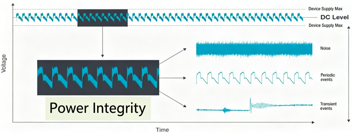
We focus on both DC and AC components when designing PDN.
The DC component is expressed as △V=△I×R. There is series resistance from VRM to IC, which causes voltage drop when DC current passes through. For example, if a current of 1A flows from VRM to the load and the line resistance is 10mΩ, a voltage drop of 1×0.01=0.01V will be generated, which is commonly referred to as IR drop. The load current is not a fixed value but changes continuously, so IR drop is also a variable value. For example, when the load operates at 2A, a voltage drop of 2×0.01=0.02V will be generated, which is very similar to the LDO routing introduced in the previous article.
However, the load does not operate stably at a single current value. For example, when playing games, the CPU performs various complex operations and the GPU performs complex rendering. The switches inside these chips operate at high speed, making the current drawn from the power supply complex. Analyzing such complex time-varying current cannot rely on resistance alone, and a parameter related to time and frequency must be introduced, namely impedance Z (Impedance = Resistance + Capacitive Reactance + Inductive Reactance). Voltage fluctuations are caused by current fluctuations.
Returning to the classic calculation formula △V=△I×R, it is slightly modified to △V=△I×Z. R is a constant independent of frequency, while Z is frequency-dependent. △V is the voltage variation caused by current change. If △V is too large and exceeds the allowable voltage fluctuation of the load, it is dangerous. Usually, the allowable voltage fluctuation of the load is 5% or 3% of the typical value (subject to the manual of the actual load), so the voltage fluctuation must not exceed 5% or 3%. For example, in the figure below, the load requires a voltage of 0.75V. Assuming the maximum allowable voltage fluctuation of the load is 3%, the maximum acceptable voltage fluctuation is 0.75×0.03=0.0225V, while the actual voltage fluctuation is only 0.015V, which meets the load demand.
Looking at the formula △V=△I×Z again, a simple transformation gives the following formula:
Ztarget = △Vmax / △Imax
As long as the actual PDN impedance Z of the circuit is sufficiently small, the voltage fluctuation caused by current fluctuation (△I×Z) will be less than △Vmax, and this impedance is the target impedance Ztarget. Therefore, the principle of PDN design is to optimize the impedance Z on the link to be lower than the target impedance Ztarget, so as to ensure that the voltage meets the load demand. In short, power fluctuation is constrained by constraining impedance. We need to know the target impedance, the specific models of capacitors on the line, and accurate simulation to obtain a reliable design.
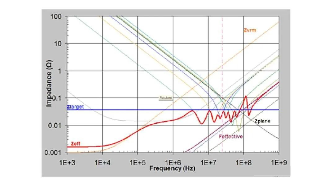
For example, the figure above shows the impedance-frequency curve. If the load operates at a single frequency and the operating current is a sinusoidal current of a single frequency, impedance optimization becomes simple—only the impedance at this frequency needs to be lower than the target impedance. However, the actual situation is complex, and we do not know the specific operating frequency. Therefore, for safety, we control the impedance within a certain frequency band instead of DC or single-frequency impedance. This may seem like over-design, but it is indeed a very safe design. The blue curve is our target impedance. What we need to do is optimize the PDN impedance within this frequency band (within Feffective frequency) so that the actual red impedance is lower than the target blue impedance within the frequency band required by the load.
The basic concepts and principles of PDN are introduced here. The next section will introduce relevant PDN optimization strategies to guide actual PCB layout, routing and capacitor selection optimization.
About Maxipcb
Maxipcb enables advanced electronic innovation. We deliver one-stop solutions including circuit design, simulation, testing, PCB fabrication, component sourcing and SMT&PCBA assembly, to boost R&D efficiency, speed up mass production and control full-cycle risks. We serve global sectors like communication, industrial automation, aerospace, automotive and semiconductor, jointly forging a safer, connected intelligent future.


