In the meticulous field of circuit design, even the tiniest error can have incalculable consequences.
Engineers must conduct a thorough and careful review of every step after completing the design.
Last week, a colleague finished his board design and sent it for prototyping. During wave soldering, a 4‑pin header could not be inserted. The SMT assembly factory reported that the SOIC‑8 power IC on the backside was overlapping with the header, making insertion impossible.
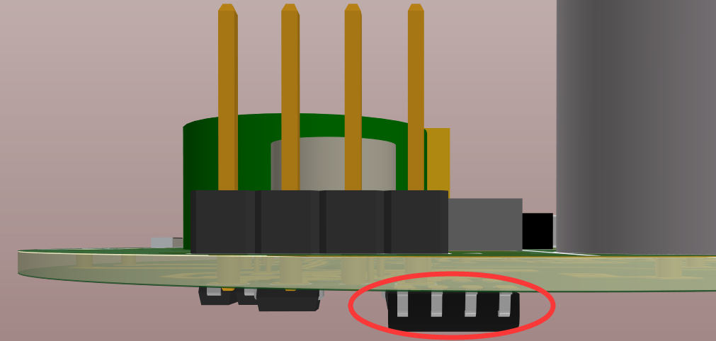
Overlapping component interference diagram (front/back view)
He was designing a compact PCB with extremely tight space constraints. Although he successfully integrated multiple complex functional modules into the limited area, he overlooked the positional relationship of components on the PCB backside during layout, which affected power access and normal operation of the entire system.
He eventually found a workaround:
First, grind down the blocked header pins slightly so they could fit. Then remove the power IC, solder the shortened header manually, and re‑solder the power IC. The process was tedious, but at least it avoided re‑prototyping.
This case highlights the critical importance of rigor and comprehensiveness in circuit design. While pursuing technological breakthroughs and innovation, engineers must maintain precise control over every detail to ensure potential issues are anticipated and resolved in the design phase.
Only in this way can the final product fully deliver its designed performance, meet real‑world application requirements, and avoid incalculable losses from careless mistakes.
Afterward, I recommended a powerful inspection tool to him: Huaqiu DFM software. It not only detects design flaws but also prevents manufacturing risks in advance and verifies whether the PCB is suitable for fabrication and assembly.
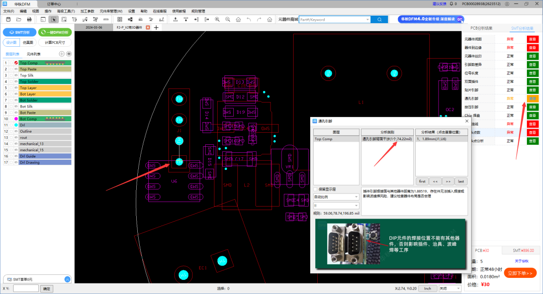
DFM software interface – SMT analysis entry
He was skeptical at first, so I imported his design file into Huaqiu DFM and ran an SMT analysis. The software immediately flagged an “interference” issue on the backside of through‑hole pins under the through‑hole pin check item.
It cut his inspection effort and time in half. He called it a lifesaver.
This reminded me of another story I heard from a senior repair technician. He once repaired a board where a small resistor was burned out, but half the resistor was blocked by a digital tube. To fix it, he had to remove the digital tube first—a high‑risk procedure that could easily damage the display.
I immediately knew the designer had placed the resistor under the digital tube to save space and simplify routing, with no regard for later maintenance. The technician had no choice but to carefully remove the digital tube.
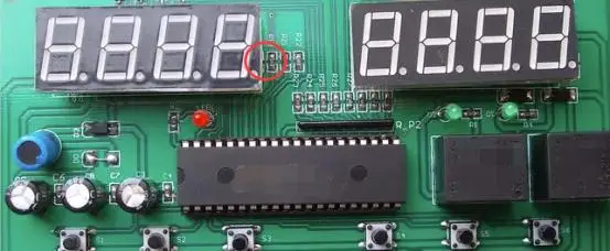
Component coverage problem – resistor hidden under digital tube
Therefore, we must think comprehensively during design. Do not cut corners and create trouble for later repair, as that leads to even greater losses. PCB layout demands extreme care—there is no room for carelessness.
To verify, I created a test case and imported it into Huaqiu DFM for SMT assembly analysis. Sure enough, the software showed a red alert under the “component spacing” check item, indicating insufficient clearance and marking the exact location.
DFM – component spacing error warning screenshot
Mistakes are unavoidable in electronic product design, but with sufficient care and the right inspection tools, design quality can be guaranteed, and even zero‑error prototyping is achievable.
About Maxipcb
Maxipcb empowers innovators to turn cutting-edge technologies into reality.
We offer one-stop solutions for design, simulation, testing, PCB manufacturing, component procurement and SMT assembly, enabling efficient development, rapid deployment and risk control across the full product lifecycle.Serving the world in communications, industrial automation, aerospace, automotive, semiconductor and beyond, we build a safer, more connected future together.


