USB is the abbreviation of Universal Serial Bus. It is a serial bus standard for connecting external devices, as well as a technical specification for input and output interfaces. It is widely used in information and communication products such as personal computers and mobile devices, and extended to other related fields including photographic equipment, digital TV (set-top boxes), game consoles, etc.
USB is the abbreviation of Universal Serial Bus. It is a serial bus standard for connecting external devices, as well as a technical specification for input and output interfaces. It is widely used in information and communication products such as personal computers and mobile devices, and extended to other related fields including photographic equipment, digital TV (set-top boxes), game consoles, etc.
The USB2.0 interface has a transmission rate of up to 480Mbps, while USB3.0 has a maximum transmission bandwidth of up to 5Gbps and introduces full-duplex data transmission. There are corresponding design requirements for the layout and routing of USB interfaces.
The pin definitions of USB2.0 and USB3.0 interfaces are shown in Figure 1.
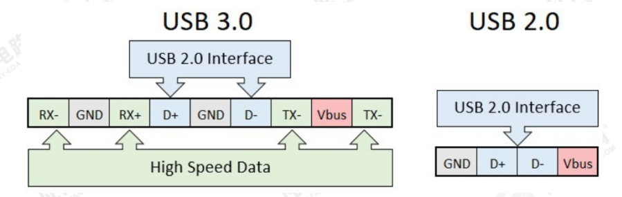
Figure 1 Pin Definitions of USB 2.0 and USB 3.0 Interfaces
I. PCB Layout Requirements for USB Interfaces
- The USB interface shall be placed close to the board edge or structural positioning, with a certain position protruding from the board edge (except for through-hole types), to facilitate plugging and unplugging.
- ESD and common mode inductor components shall be placed close to the USB interface, in the order of ESD → common mode inductor → resistor and capacitor.
- Attention shall be paid to the distance between the ESD device and the USB interface, with a certain spacing reserved to take into account the post-soldering process.
- During layout, the differential line length shall be minimized as much as possible to shorten the distance of the differential pair.
II. PCB Routing Requirements for USB Interfaces
- USB signals must be routed as differential pairs, with impedance controlled at 90 ohms and ground wrapping treatment applied. The total length should preferably not exceed 1800mil.
- Minimize the trace length as much as possible, and give priority to the routing of high-speed USB differential pairs (RX and TX differential pairs). When routing USB differential traces, minimize the number of layer transition vias as much as possible, to achieve better impedance control and avoid signal reflection.
- Vias will cause impedance discontinuity of the line. A pair of return ground vias shall be added at each layer transition position via drilling for signal return during layer switching.
- If the positioning posts on both sides of the USB are connected to the protective ground, ensure a distance of 2mm from the signal GND during plane splitting, and place multiple vias in the protective ground area to ensure sufficient connection, as shown in Figure 2.
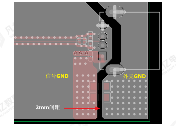
Figure 2 Isolation Between Chassis GND and Signal GND
- Due to factors such as pin distribution, vias and routing space, the length of differential lines is prone to mismatch. Once the routing length is mismatched, timing deviation will occur, which will also cause common mode interference and reduce signal quality. Therefore, corresponding compensation shall be made for the mismatch of the differential pair to achieve line length matching. The length difference is usually controlled within 5mil, and the compensation shall be carried out in accordance with the differential length matching specification.
The comparison of PCB routing requirements between USB2.0 and USB3.0 is shown in Table 1 below.
Table 1 PCB Routing Requirements for USB2.0 and USB 3.0
| Parameter |
USB2.0 Requirements |
USB3.0 Requirements |
| Routing Impedance |
Differential 90ohm±10% |
Differential 90ohm±10% |
| Maximum Intra-pair Delay Difference of Differential Pair |
<20mil |
<6mil |
| Routing Length |
<6 inches |
<6 inches |
| Maximum Allowed Number of Vias per Signal |
Recommended no more than 4, must not exceed 6 |
Recommended no more than 2 |
| Capacitor Requirements |
- |
100nF+20%, 0201 package recommended |
| Spacing Between Differential Pairs |
- |
Recommended ≥4 times the USB trace width |
| Spacing Between USB and Other Signals |
- |
Recommended ≥4 times the USB trace width |
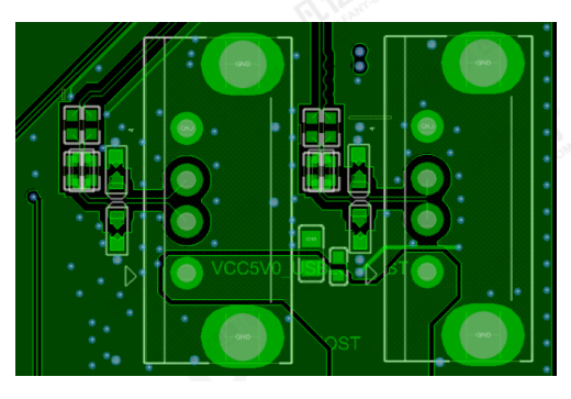
Figure 3 Layout and routing of USB 2.0
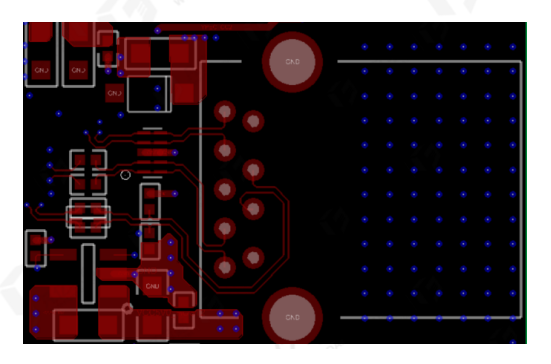
Figure 4 Layout and Routing of USB 3.0
III. PCB Design for Type C Interface
USB Type C, also known as USB-C. It should be noted that Type-C is only an interface form and has no relation to the USB version. The highlights of this interface include a slimmer design, faster transmission speed (up to 10Gbps) and more powerful power transmission (up to 100W). The biggest feature of the Type-C double-sided pluggable interface is that it supports double-sided insertion of the USB interface, which is mainly for thinner and slimmer devices. The pin definition of the Type-C interface is shown in Figures 7-23 below.
Figures 7-23 Pin Definition of Type C Interface
PCB Design Requirements for Type C Interface:
- ESD and common mode inductor components shall be placed close to the Type C interface, in the order of ESD → common mode inductor → resistor and capacitor. Attention shall also be paid to the distance between the ESD device and the Type C interface, with a certain spacing reserved to take into account the post-soldering process.
- The coupling capacitors of TX signal lines shall be placed close to the interface, and the coupling capacitors of RX signal lines are provided by the device end, as shown in Figures 7-24.
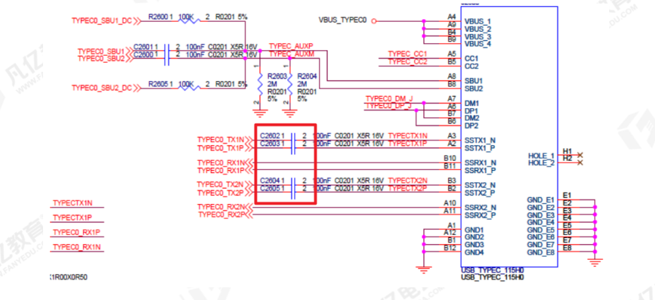
Figures 7-24 Coupling Capacitors for TX Signal Lines
- The impedance of Type C differential traces is controlled at 90ohm±10%. To ensure impedance continuity, a complete reference plane shall be provided without crossing plane splits, and the number of layer transition vias for signal routing shall not exceed 2.
- Type-C has four groups of differential signals (RX/TX1-2) and two groups of differential signals (D+/D-), totaling six differential pairs. The differential signal lines are required to be adjacent to at least one ground plane, preferably adjacent to ground planes on both sides. The traces shall be as short as possible, with the maximum length not exceeding 6 inches.
- Ensure the length matching of Type C differential lines, with the intra-pair length matching error <6mil, and the length matching shall be carried out in accordance with the differential length matching specification.
- To avoid the impact between Type C differential pairs or between differential pairs and other signals, the spacing between pairs is recommended to be ≥4 times the Type C trace width, and the spacing from other signals shall be kept ≥4 times the Type C trace width as much as possible.
- CC1/CC2 are two key pins with multiple functions: connection detection, front and back side identification, DFP and UFP distinction (i.e., master-slave configuration), and Vbus configuration. The traces shall be widened during routing.
Note: When the operating rate of the Type-C connector is ≥8Gbps, the design shall be processed in accordance with the connector optimization recommendations in Section 5.6 of Chapter 5.
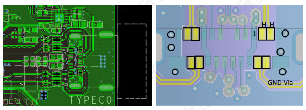
Figure 7-25 Routing Schematic of Type-C Connector
About Maxipcb
Maxipcb empowers innovators to turn cutting-edge technologies into reality.
We offer one-stop solutions for design, simulation, testing, PCB manufacturing, component procurement and SMT assembly, enabling efficient development, rapid deployment and risk control across the full product lifecycle.Serving the world in communications, industrial automation, aerospace, automotive, semiconductor and beyond, we build a safer, more connected future together.

 Figure 1 Pin Definitions of USB 2.0 and USB 3.0 Interfaces
 Figure 2 Isolation Between Chassis GND and Signal GND

 Figures 7-24 Coupling Capacitors for TX Signal Lines
 Figure 7-25 Routing Schematic of Type-C Connector