This paper introduces the common drilling problems in PCB sketchpad to avoid stepping on the same pit in the future.
This paper introduces the common drilling problems in PCB sketchpad to avoid stepping on the same pit in the future. Boreholes are divided into three categories: through holes, blind holes and buried holes. No matter what kind of holes, the problem of missing holes will directly lead to the unavailability of the whole batch of products. Therefore, the correctness of drilling design is particularly important.
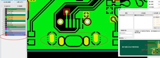
Case explanationQuestion 1: The file slot designed by 1:Altium is misplaced; Description of the problem: the slot hole is missing, and the product cannot be used. Cause analysis: the design engineer missed the slot of USB device when making the package. When drawing the board, he found this problem and did not modify the package, but directly drew the slot on the hole symbol layer. Theoretically, there is not much problem in this operation, but in the manufacturing process, only the drilling layer is used for drilling, so it is easy to ignore the existence of slots in other layers, which leads to the omission of drilling in this slot and the product can not be used. Please see the picture below;
How to avoid pits: Each layer of PCB design documents has its own function. Drilling holes and slots must be placed in the drilling layer, and it cannot be considered that the design can be made.
 Question 2: Altium designed file via 0 D code;
Problem description: The drain hole is open and non-conductive. Cause analysis: Please see Figure 1. There is a leak in the design document. When DFM manufacturability is checked, the leak is indicated. After the cause of the leak was investigated, the hole size was checked in Altium software, and the hole diameter of the leak hole was 0, resulting in no hole in the design file. Please see Figure 2.
The reason for this leak is the design engineer's misoperation when drilling holes. If the problem of this leak is not investigated, it is difficult to find that there is a leak in the design document, which directly affects the electrical failure and the designed product cannot be used.
How to avoid the pit: DFM manufacturability test must be carried out after the circuit diagram design is completed, and the leakage hole cannot be found in the manufacturing and production during the design. DFM manufacturability test before manufacturing can avoid this problem.
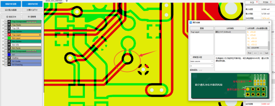
Figure 1: Leaks in Design Documents
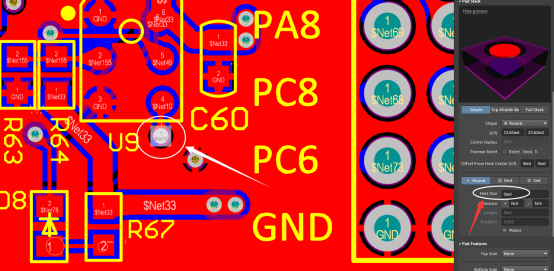
Figure 2: Altium pore size is 0.
Question 3: The file designed by 3:PADS can't be exported through the hole; Problem description: The drain hole is open and non-conductive.Cause analysis: Please see Figure 1. There are many leaks when using DFM manufacturability test. After investigating the causes of the leakage problem, one group of vias in PADS is designed as semi-vias, which leads to the design file not outputting semi-vias, resulting in leakage, as shown in Figure 2. There is no semi-conductive hole in the double panel, and the engineer mistakenly set the via hole as a semi-conductive hole in the design, and the semi-conductive hole was leaked during the output drilling, resulting in leakage.
How to avoid the pit: this kind of misoperation is not easy to find. DFM manufacturability analysis and inspection should be carried out after the design is completed, and problems should be found before manufacturing to avoid leakage.
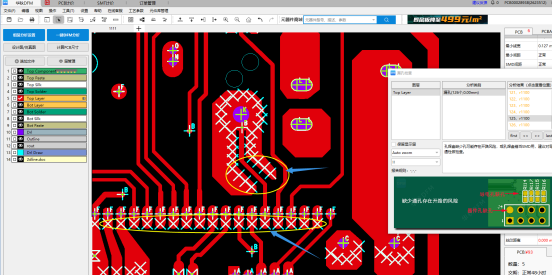
Figure 1: Leaks in Design Documents
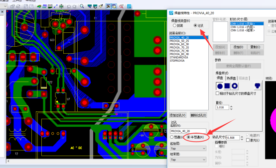
Figure 2: PADS software dual-panel vias are semi-vias.
Question 4: allegro's Gerber file is leaking;Problem description: HDMI device has a pin hole, so it cannot be plugged in.
Cause analysis: Please look at Figure 1, and indicate the leak when using DFM for manufacturability inspection. After checking the cause of the leakage problem, the output Gerber file lacks slot layers, which is caused by the output drilling, and the output slot layers are not continuously exported, which leads to the leakage. Please see Figure 2.
Similar to HDMI device, the pin of the device can't be inserted if it leaks into the slot hole. This pin generally has a ground network, which will lead to an open circuit if the multi-layer board is used to fill the slot.
How to avoid the pit: this problem is easy for beginners to forget the output slot hole layer, so DFM must be used for manufacturability inspection before plate making to avoid the problem of slot hole leakage.
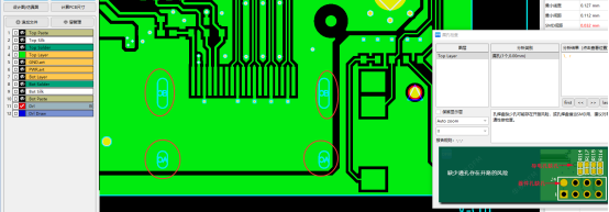
Figure 1: Leaky slot hole
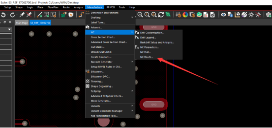
Figure 2: Output ROU layer
Conclusion:The holes in PCB circuit board design are very important. The wiring needs to be punched, the structure needs to be punched with positioning holes, and the DIP device needs to be punched with plug-in holes. If the design leaks, the whole design will fail.
About MaxipcbMaxipcb inspires and empowers innovators and helps them bring world-changing technologies to life. We provide advanced design, simulation and testing solutions to help engineers complete development and deployment faster in the whole product life cycle, while controlling risks. Our customers are all over the world, such as communication, industrial automation, aerospace and national defense, automobile, semiconductor and general electronics. We join hands with customers to accelerate innovation and create a safe and interconnected world. 