LDO stands for Low Drop-Out, also known as a low-dropout regulator. It is an electronic component mainly used to step down high voltage to a lower voltage and provide stable power supply. An LDO module usually consists of a DC voltage regulator and a current amplifier. Its working principle is to create a stable voltage difference between the input and output to ensure the output voltage stays within a reliable range.
LDO stands for Low Drop-Out, also known as a low-dropout regulator. It is an electronic component mainly used to step down high voltage to a lower voltage and provide stable power supply. An LDO module usually consists of a DC voltage regulator and a current amplifier. Its working principle is to create a stable voltage difference between the input and output to ensure the output voltage stays within a reliable range.
Features of LDO modules:
- Low dropout voltage: The dropout voltage of an LDO module is typically between hundreds of millivolts and several volts, so it can step down high voltage to a lower level.
- Stability: The LDO module delivers a stable output voltage unaffected by input voltage fluctuations, with good noise immunity and anti-interference performance.
- Low power consumption: Using a linear regulator topology, the LDO module does not require frequent switching, resulting in low power consumption.
- Fast response: The LDO module features fast response and can quickly adjust the output voltage to adapt to load changes.
LDO modules are widely used in electronic devices such as mobile devices, communication equipment, and embedded systems to provide stable voltage for various circuits and chips.
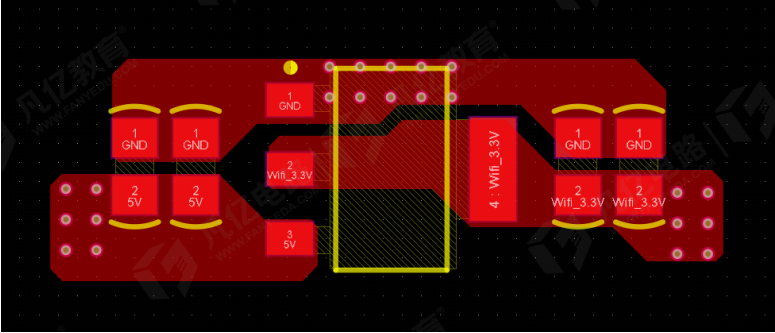
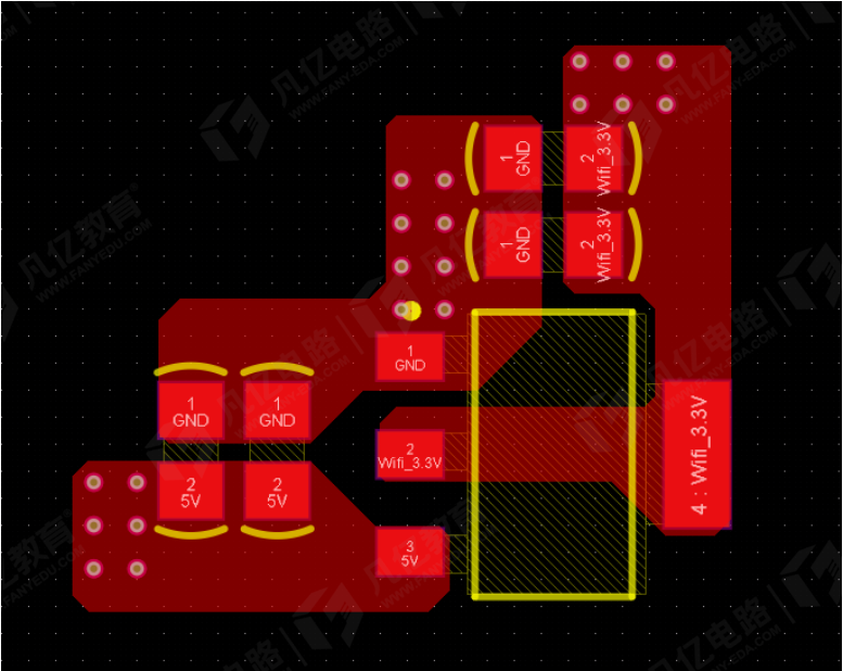
Key Points of LDO PCB Layout
- Analyze power input and output; adopt an in-line layout or L-type layout, and minimize the power loop area as much as possible.
- Arrange input and output filter capacitors in the order of large capacitance first, small capacitance later.
Key Points of LDO PCB Routing
- Power paths and the number of vias shall meet the current-carrying requirements.
- Power input vias shall be placed before the first filter capacitor; power output vias shall be placed after the last filter capacitor.
- GND current-carrying paths shall be sufficiently wide, and all vias shall be placed close to the chip GND pins.
- Input ground and output ground shall be connected together to ensure a robust return current path.
 About Maxipcb
Maxipcb enables advanced electronic innovation. We deliver one-stop solutions including circuit design, simulation, testing, PCB fabrication, component sourcing and SMT&PCBA assembly, to boost R&D efficiency, speed up mass production and control full-cycle risks. We serve global sectors like communication, industrial automation, aerospace, automotive and semiconductor, jointly forging a safer, connected intelligent future.


