In the electronics industry, protecting equipment against Electrostatic Discharge (ESD) is essential. ESD refers to a very high voltage spike that can easily damage small-signal components such as integrated circuits and low-power semiconductors. Common ESD is caused by human contact with electronic devices: electric charges accumulate in the human body, and discharge when the body touches the device, accompanied by an extremely high voltage spike.
The following introduces how to reduce ESD damage in PCB design:
1. Use Clamping Diodes
Clamping diodes are most commonly used in integrated circuits to protect devices from ESD damage. Microcontrollers, digital signal controllers and processors are equipped with internal ESD clamping diodes. However, low-cost controllers may lack internal clamping diodes, in which case an external clamping diode needs to be added close to the device. The figure below shows the inherent ESD clamping diodes of an IC.
 Inherent ESD clamping diodes of an IC
During normal operation, assuming the voltage of Pin 1 is expected to be between 0-3.3V, D1 and D2 will not interfere with the circuit. When the high level is 3.3V, D1 is reverse biased and non-conducting; D2 is also non-conducting because its cathode is connected to VCC and the high level of the pin is equal to VCC. When the voltage of Pin 1 is 0, D2 is reverse biased and D1 is unbiased.
In the presence of a high voltage spike caused by ESD, the diodes will conduct. For example: if the spike is extremely high, D2 will be forward biased and the spike will be diverted to VCC, thus protecting the internal components of the IC. In the presence of a very high negative spike, D1 will conduct and divert the spike to the ground.
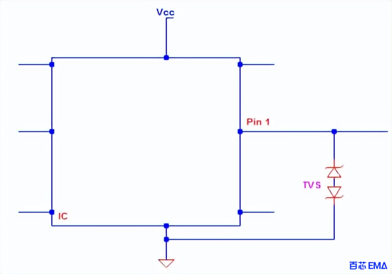
It is critical to confirm whether the IC you use has built-in ESD protection. If not, add an external clamping diode as shown in the figure below:
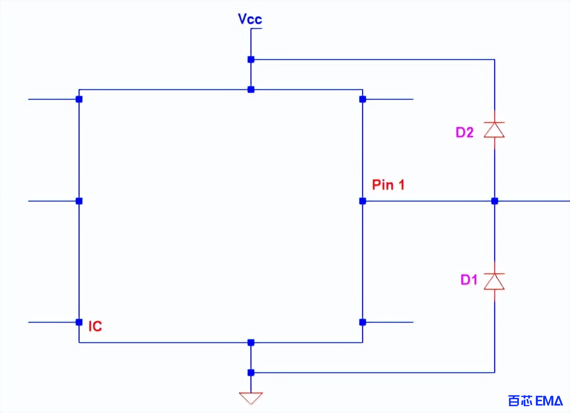 External ESD clamping diode for an IC
It is certainly not feasible and highly costly to add clamping diodes to all pins of an IC. Generally, after a product is manufactured and enclosed in a housing, the IC will not be accessible, and only a small number of characteristic pins require clamping diode protection. Silicon diodes or Schottky diodes can be used as clamping diodes.
The following are the most common pins that usually require clamping diode protection:
- Programming pins: Generally used by engineers. Some products require on-site reprogramming, making programming pins highly susceptible to ESD. Another reason for adding clamping diodes to programming pins is compliance—if you sell your products, you must comply with ESD standards. In ESD testing, voltage spikes are intentionally injected into exposed pins, and the product must not be damaged.
- Reset pins: It is undesirable for a product to reset or restart without reason. Reset pins are often accessible externally, and ESD may cause the device to restart or be permanently damaged. Reset pins may be interfered with during other compliance tests such as surge tests, leading to device restart—which is an unwanted outcome (although this is not an ESD scenario, the high level of surge voltage spikes is equivalent to simulating ESD).
- IC pins for detecting line voltage or higher DC voltage: These pins are actually not accessible externally, so the probability of ESD on them is low. However, they may encounter higher voltage spikes during surge testing or actual surges, which are essentially similar to ESD. Experience shows that such spikes can easily cause ESD damage.
2. Use Transient Voltage Suppressors (TVS)
TVS diodes are fast-acting clamping diodes, different from ordinary PN junction diodes such as the aforementioned clamping diodes. TVS diodes have similar functions and effects to clamping diodes: they clamp the voltage once the breakdown voltage is reached, otherwise they remain open-circuited.
The figure below shows common TVS symbols: Figure A and B are bidirectional TVS diodes, and Figure C is a unidirectional TVS diode. Bidirectional TVS diodes can block positive or negative ESD spikes, while unidirectional ones can only suppress spikes in one direction.
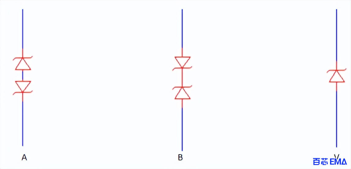 Common TVS Diode Symbols
The following three figures show example connections for using TVS diodes to protect specific pins from ESD:
-
Unidirectional TVS diode mounted on an IC pin
The TVS diode is non-conducting during normal circuit operation. When a positive spike occurs, the device clamps the voltage; when a negative spike occurs, the device is forward biased and diverts the spike to the ground.
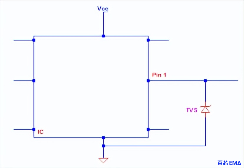 Unidirectional TVS Diode Mounted on an IC Pin
-
Bidirectional TVS diode (Connection 1)
The TVS diode does not interfere with the circuit during normal operation. It clamps the voltage and protects the IC during positive or negative voltage spikes.
 Bidirectional TVS Diode (Connection 1)
-
Bidirectional TVS diode (Connection 2)
The TVS diode does not interfere with the circuit during normal operation. It clamps the voltage and protects the IC during positive or negative voltage spikes.
 Bidirectional TVS Diode (Connection 2)
3. Use Zener Diodes
Using Zener diodes for ESD protection follows the same principle as unidirectional TVS diodes. The disadvantages of Zener diodes are that they are slower than TVS diodes and can only handle lower energy at the same package size. A larger Zener diode is required to withstand higher energy, which takes up more PCB space and increases costs.
4. Use High-Frequency Capacitors
In automotive circuit design, the human body is assumed to have an equivalent capacitance of 300pF, which can store a potential of up to 8kV. When a person touches an object, the charge in the body discharges, which can damage small electronic devices.
The following setup shows how a capacitor mounted on an IC pin provides ESD protection: when the human body touches the pin, the human body's capacitance is in parallel with the ESD protection capacitor. As a result, the 8kV potential in the human body is suppressed.
Based on the law of conservation of charge, the final charge equals the initial charge. Treating the human body as the initial charge source:
Qinitial=CHumanBody×VHumanBody
Initial Charge Calculation
When the human body touches the ESD-exposed pin, charging occurs, and:
Qfinal=Vfinal×Cfinal
Final Charge Calculation
According to the law of conservation of charge (
Qinitial=Qfinal), where
Cfinal is the parallel combination of
CESD and the human body capacitance, and
Vfinal is the actual voltage the capacitor withstands:
Vfinal×Cfinal=CHumanBody×VHumanBody
Vfinal=CfinalCHumanBody×VHumanBody
Vfinal=CESD+CHumanBodyCHumanBody×VHumanBody
Conservation of Charge Formula
As mentioned above,
VHumanBody=8kV and
CHumanBody=330pF. Assuming a
CESD of 33nF is selected, the final voltage is:
Vfinal=33nF+330pF330pF×8kV=79.2V
Final Voltage Calculation
Therefore, after installing a 33nF ESD protection capacitor on the pin, the voltage the pin withstands is only 79.2V instead of 8kV. The rated voltage of the capacitor must be higher than this value. To further reduce the voltage level, simply increase the ESD capacitor value—however, this will also increase the PCB size.
The above are 4 methods to protect equipment from ESD damage. You can choose any of them, as each has its advantages and disadvantages in practical applications, and their effectiveness must be verified through actual testing.
Optimized PCB design can reduce unnecessary troubleshooting and rework costs. The following are additional measures to prevent ESD in PCB design:
5. Reduce Circuit Loop Area
Current is induced in a closed circuit loop with varying magnetic flux, and the amplitude of the induced current is proportional to the loop area. In other words, the loop area must be minimized—
the larger the loop, the greater the magnetic flux, and the stronger the induced current in the circuit. This also reduces the high-frequency EMI electromagnetic field generated by ESD pulses.
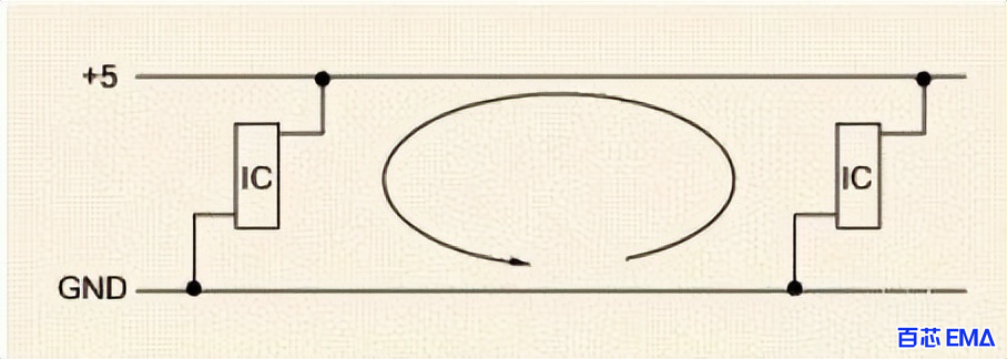 Reducing Circuit Loop Area
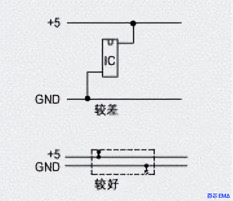
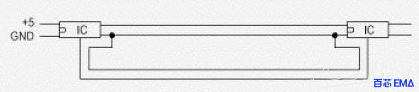
The most common loop is the one between the power supply and ground as shown in the figure above. If a multi-layer PCB cannot be used, the power and ground lines must be connected in a grid as shown below:
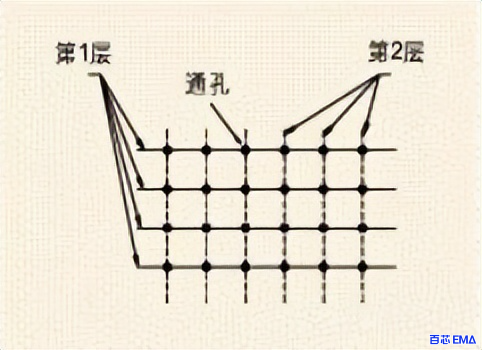 Power and Ground Lines Connected in a Grid (Dual-Layer PCB)
Grid connection can act as power and ground planes, with traces on each layer connected via vias. The spacing between connected vias should be within 6cm in all directions. In addition, routing power and ground traces as close as possible can also reduce the loop area:
 Power and Ground Traces Routing (Poor vs. Good Practice)
Another method to reduce loop area and induced current is to minimize parallel paths between interconnected devices:
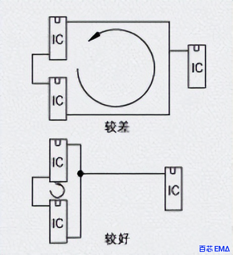 Minimizing Parallel Paths Between Interconnected Devices (Poor vs. Good Practice)
When signal connection lines longer than 30cm must be used, guard traces can be added:
 Using Guard Traces for Long Signal Lines
A better method is to route ground traces within 13mm of signal lines (on guard traces or ground planes), with a ground trace paired with each long signal line (>30cm) for sensors or power supplies:
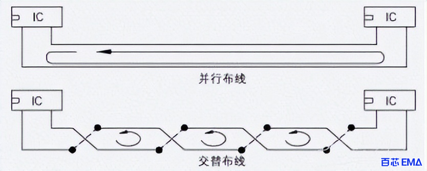 Routing Ground Traces Adjacent to Long Signal Lines (Parallel vs. Alternating Routing)
6. Minimize Trace Length
Long signal traces can act as antennas to receive ESD pulse energy. Using shorter signal traces reduces the efficiency of the traces as antennas for receiving ESD electromagnetic fields. Interconnect devices at adjacent positions to minimize the length of interconnection traces.
7. Reduce Charge Injection
Direct ESD discharge to the ground plane may damage sensitive circuits. Therefore, when using transient diodes, it is best to place one or more high-frequency bypass capacitors between the power supply and ground of vulnerable components.
Bypass capacitors reduce charge injection and maintain the voltage difference between the source and ground ports. TVS diodes shunt induced current and maintain the voltage difference across the TVS clamp. TVS diodes and capacitors should be placed as close as possible to the protected IC to ensure the shortest path from the TVS diode to the ground and minimize trace length, thus reducing parasitic capacitance effects.
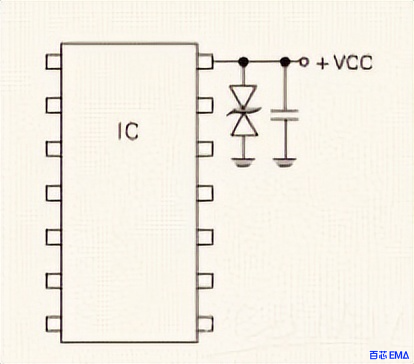 Reducing Charge Injection with Bypass Capacitors and TVS Diodes
Connect to the copper layer that must be mounted on the PCB. Ideally, the copper layer should be isolated from the PCB contact layer and connected to the pad via short wires.
8. Other Additional Measures
- Avoid routing important signal lines (e.g., clock, reset signals) near PCB edges;
- Set unused areas of the PCB as ground planes;
- Keep the main housing ground line at least 4mm away from signal lines;
- Maintain an aspect ratio of less than 5:1 for the main housing ground line to reduce inductive effects;
- Protect all external connections with TVS diodes.
About Maxipcb
Maxipcb empowers innovators to turn cutting-edge technologies into reality.
We offer one-stop solutions for design, simulation, testing, PCB manufacturing, component procurement and SMT assembly, enabling efficient development, rapid deployment and risk control across the full product lifecycle.Serving the world in communications, industrial automation, aerospace, automotive, semiconductor and beyond, we build a safer, more connected future together.

 Inherent ESD clamping diodes of an IC
 External ESD clamping diode for an IC
 Common TVS Diode Symbols
 Unidirectional TVS Diode Mounted on an IC Pin
 Bidirectional TVS Diode (Connection 1)
 Bidirectional TVS Diode (Connection 2)
 Reducing Circuit Loop Area
 Power and Ground Lines Connected in a Grid (Dual-Layer PCB)
 Power and Ground Traces Routing (Poor vs. Good Practice)
 Minimizing Parallel Paths Between Interconnected Devices (Poor vs. Good Practice)
 Using Guard Traces for Long Signal Lines
 Routing Ground Traces Adjacent to Long Signal Lines (Parallel vs. Alternating Routing)