Through-hole vias act as conductive structures for connecting traces on different layers of a multilayer printed circuit board (PCB).
Through-hole vias act as conductive structures for connecting traces on different layers of a multilayer printed circuit board (PCB).
At low frequencies, vias do not affect signal transmission. However, as frequency increases (above 1 GHz) and signal rise edges become steep (as fast as 1 ns), vias can no longer be regarded simply as electrical connections; the impact of vias on signal integrity must be carefully evaluated. Vias behave as impedance-discontinuity breakpoints on transmission lines, resulting in signal reflection.
Nevertheless, the problems caused by vias are mostly concentrated in parasitic capacitance and parasitic inductance. The primary effect of via parasitic capacitance on a circuit is to prolong the signal rise time and reduce the operating speed of the circuit.
In contrast, parasitic inductance weakens the effectiveness of bypass circuits and degrades the filtering performance of the entire power supply system.
1. Impact of Through-Hole Vias on Impedance Continuity
Based on Time Domain Reflectometer (TDR) curves with and without vias, significant signal delay occurs in the presence of vias.
The signal propagation time span to the second test point is 458 ps without vias, compared to 480 ps with vias. Thus, vias introduce a signal delay of 22 ps.
Signal delay is mainly caused by the parasitic capacitance of the via, which can be calculated using the following formula:
In this formula:
- D₂ refers to the antipad diameter on the ground layer (mm)
- D₁ refers to the via pad diameter (mm)
- T is the PCB thickness (mm)
- εᵣ is the dielectric constant of the reference layer
- C is the parasitic capacitance (pF)
In this analysis, the via length is 0.96 mm, via diameter is 0.3 mm, pad diameter is 0.5 mm, and dielectric constant is 4.2. Substituting these values into the formula yields a parasitic capacitance of approximately 0.562 pF.
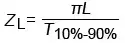
For a 50 Ω signal transmission line, this via causes a change in the signal rise time, calculated using the following formula:
Using the formula above, the rise time variation caused by via capacitance is 30.9 ps, which is 9 ps longer than the measured result (22 ps), indicating a discrepancy between theoretical and actual values.
In summary, the signal delay caused by via parasitic capacitance is not significant.
However, in high-speed circuit design, special attention must be paid to via usage for layer transitions in routing.
Compared with parasitic capacitance, the parasitic inductance of vias causes more severe circuit degradation. The parasitic inductance of a via can be calculated using the following formula:
In this formula:
- L represents the parasitic inductance of the via (nH)
- h represents the via length (mm)
- d represents the via diameter (mm)
The equivalent impedance caused by via parasitic inductance can be calculated using the following formula:
The test signal has a rise time of 500 ps, with a calculated equivalent impedance of 4.28 Ω. However, the measured impedance change caused by the via exceeds 12 Ω, showing a substantial difference between measured and theoretically calculated values.
2. Impact of Via Diameter on Impedance Continuity
A series of experiments leads to the conclusion that the larger the via diameter, the greater the impedance discontinuity.
In high-frequency, high-speed PCB design, impedance variation is typically controlled within ±10% to avoid signal distortion.
3. Impact of Pad Size on Impedance Continuity
Parasitic capacitance strongly affects resonant points within the frequency band of high-speed signals, causing bandwidth offset. The main factor influencing parasitic capacitance is pad size, which correspondingly impacts signal integrity. Therefore, the larger the pad diameter, the stronger the impedance discontinuity.
When the pad diameter varies from 0.5 mm to 1.3 mm, the impedance discontinuity caused by the via decreases continuously. The impedance changes significantly when the pad size increases from 0.5 mm to 0.7 mm; as pad size increases further, the variation in via impedance becomes gradual. Thus, a larger pad diameter reduces the impedance discontinuity caused by the via.
4. Return Path of Via Signals
The fundamental principle of return signal flow is that high-speed return current flows along the path of least inductance.
Since a PCB contains more than one ground plane, return signal current flows directly along the path on the ground plane closest to the signal trace. When all signal current flows on the same plane from one point to another, the return current does not jump—unless the signal switches layers through a via.
In high-speed PCB design, a proper return path can eliminate impedance mismatch. Ground vias can be placed around signal vias to provide a return path for signal current and form an inductive loop between signal vias and ground vias. Even if impedance discontinuity occurs due to via effects, current can flow through the inductive loop, thereby improving signal quality.
5. Signal Integrity of Through-Hole Vias
S-parameters can be used to evaluate the impact of vias on signal integrity, characterizing all components of a channel including loss, attenuation, reflection, and other parameters.
A series of experiments cited in this article shows that ground vias reduce transmission loss, and increasing the number of ground vias around a signal via further lowers loss. Adding ground vias around vias mitigates the loss caused by vias to a certain extent.
6. Conclusion
Conclusion 1
Impedance discontinuity caused by through-hole vias is affected by via diameter and pad size. Larger via diameter and pad diameter result in more severe impedance discontinuity. The impedance discontinuity caused by vias generally decreases as pad size increases.
Conclusion 2
Adding ground vias significantly improves via impedance discontinuity, allowing it to be controlled within ±10%. Furthermore, adding ground vias effectively enhances signal integrity.
About Maxipcb
Maxipcb empowers innovators to turn cutting-edge technologies into reality.
We offer one-stop solutions for design, simulation, testing, PCB manufacturing, component procurement and SMT assembly, enabling efficient development, rapid deployment and risk control across the full product lifecycle.Serving the world in communications, industrial automation, aerospace, automotive, semiconductor and beyond, we build a safer, more connected future together.


