What is a Mark point?
Mark point is a kind of marking point used for machine vision positioning in the process of PCB processing and mounting. It helps the mounter, welding machine and other equipment to accurately identify the position and direction of the circuit board and ensure the assembly accuracy.
What is a Mark point?Mark point is a kind of marking point used for machine vision positioning in the process of PCB processing and mounting. It helps the mounter, welding machine and other equipment to accurately identify the position and direction of the circuit board and ensure the assembly accuracy.
Foolproof design of Mark pointThe fool-proof design of Mark points refers to ensuring that Mark points are not easily mistaken for identification or installation errors in actual production and use through reasonable design and layout, thus improving accuracy and reliability.
In terms of design standards, Mark points need to be arranged diagonally to form an asymmetric pattern. Mark points on the board are placed in an L-shape with a distance of ≥6mm from the board edge. Generally, there are three points on the front side and three points on the back side, and auxiliary edges are arranged according to the process requirements. Avoid areas with dense devices. The surrounding area of 3mm must be kept clean, without other graphics, words or components, and the background is a uniform color of solder mask to ensure good optical recognition effect.
Two Mark points placed diagonally should meet the requirements of foolproof, and the distance between one Mark point and the transfer edge is greater than or equal to the distance between the other Mark point and the transfer edge plus 6mm, which is foolproof and can also avoid the 180-degree rotation error when PCB is loaded on the mounter.
Assuming that the left and right sides of PCB are transmission edges, and A&B&C is the distribution of MARK points on the board, A&B should meet the requirements of foolproof.
Assume that A is 260MIL to the transmission edge and 250MIL to the non-transmission edge.
Then B is 260MIL+240=500MIL to the transmission side, and it is enough to meet the minimum requirement of 6MM to the non-transmission side.
In general, at least the distance from it to the conveying edge should be ≥6MM.
From the technical specifications, the shape of the Mark point is usually circular (the shape can be customized for Xin MarsPCB design software), and the diameter is usually 1.0mm (it can be adjusted to 0.8mm-1.5mm according to the equipment requirements), which is flush with the PCB surface and has clear edges without burrs. The material requires bare copper, which has a smooth surface and no oxidation, showing the natural color of copper and forming a good optical contrast with the surrounding solder mask.
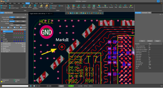
Mark points can be divided into global Mark points, local Mark points and mosaic Mark points according to their uses, and can be divided into two-point positioning, three-point positioning and single-point positioning according to their numbers. Among them, two-point positioning is the most commonly used, which can provide position and angle information, while three-point positioning is used for large PCB to provide higher accuracy.
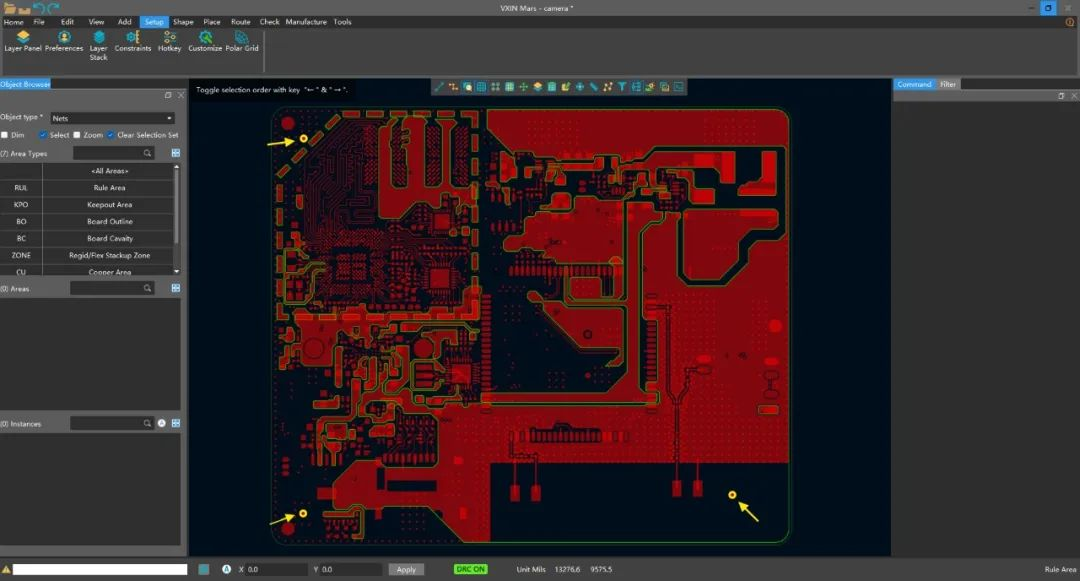
Global Mark points
Local Mark point
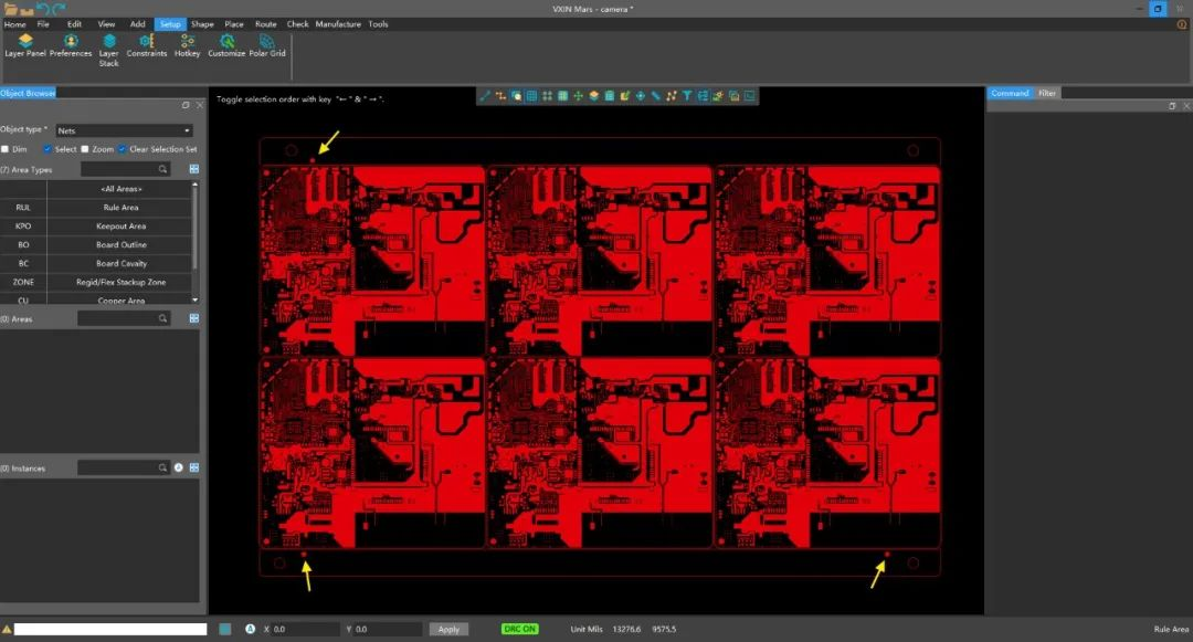
Imposition Mark point
About Maxipcb
Maxipcb empowers innovators to turn cutting-edge technologies into reality.
We offer one-stop solutions for design, simulation, testing, PCB manufacturing, component procurement and SMT assembly, enabling efficient development, rapid deployment and risk control across the full product lifecycle.
Serving the world in communications, industrial automation, aerospace, automotive, semiconductor and beyond, we build a safer, more connected future together.


