This document provides PCB design and routing guidelines for Microchip 10/100/1000 Mbps Ethernet devices, focusing on signal integrity, EMI, and ESD.
This document provides PCB design and routing guidelines for Microchip 10/100/1000 Mbps Ethernet devices, focusing on signal integrity, EMI, and ESD.
1. General PCB Routing Guidelines
Power Supply Requirements
- Ensure sufficient power rating for all regulators.
- Power output ripple: < 50 mV (preferably < 10 mV).
- Noise on power/ground planes: < 50 mV.
- Ferrite bead current rating: 4–6× the expected load (include temperature derating).
Device Decoupling
- Every high‑speed IC requires decoupling caps at each power pin.
- Typical value: 0.001 μF – 0.1 μF.
- Use Class II dielectric: X7R (first choice), X5R (second choice).
- Place caps as close to pins as possible.
- Keep leads extremely short; connect directly to top‑layer GND/power.
- Via length from pad to via: < 10 mil.
- Use two vias per capacitor ground to minimize inductance.
PCB Bypass
- Place bypass caps near all power entry points.
- Use for all power connections and regulators.
- Keep leads short; use wide traces.
- Dual vias to GND are highly recommended.
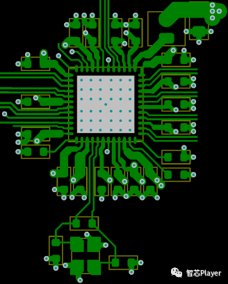
Figure 1 – PCB bypass technique example
Bulk Capacitance
- Use bulk caps to minimize switching noise and stabilize voltage.
- Place on all power planes and regulators.
- Keep connections short; use in‑pad vias if possible.
- For ferrites: place bulk caps on both sides of the bead.
- For USB VCC filtering: place 4.7 μF inside the ferrite (not on the connector side).
PCB Layer Strategy
- Minimum 4 layers for Ethernet designs.
- Recommended stackup:
- 4‑layer: Top Signal → GND → Power → Bottom Signal
- 6‑layer: Top Sig → Power/GND → Sig2 → Sig3 → GND → Sig4
- Route critical high‑speed signals adjacent to a continuous GND plane.
- Avoid crossing plane splits (causes return path disruption, SI and EMI issues).
- If crossing splits is unavoidable: add strap capacitors.
- Isolate chassis GND from digital GND.
- Eliminate ground loops.
- Route adjacent layers orthogonally to reduce crosstalk.

Figure 2 – Example of signal crossing a plane split (NOT recommended)
Signal Integrity
- Use AC termination for high‑speed clocks and switching signals (at the load end).
- Use series termination for impedance matching (at the driver end).
- Minimize vias (add inductance).
- Check for traces over plane cutouts (EMC risk).
- Maintain sufficient spacing to avoid crosstalk; use guard traces.
PCB Trace Rules
- No 90° bends on high‑speed traces (impact impedance).
- Size trace width for required current.
- Keep component leads to planes as short as possible.
Crystal Circuit
- Place all crystal components on the top layer.
- Isolate crystal circuits from other signals.
- Locate load caps, crystal, and parallel resistor close together.
- Match crystal trace lengths; keep paths short.
- Verify frequency accuracy: ±50 PPM across temperature and life.
Thermal Pad (Exposed Pad) Vias
- Fill the GND thermal pad with vias for good thermal and electrical connection.
- Use ≥ 1 oz copper ground plane.
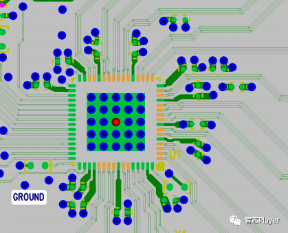
Figure 3 – Example of ground via array in thermal pad
2. Ethernet Differential Pair Routing
- Route Tx+/Tx–, Rx+/Rx– as 100 Ω controlled impedance differential pairs.
- Keep pairs tight; typical spacing: 4–5 mil.
- Isolate from other signals: ≥ 0.3 inch clearance.
- Intra‑pair skew: < 50 mil; inter‑pair skew: < 600 mil.
- Keep pairs as short as possible.
- Minimize vias and layer changes; match vias if used.
- Route pairs first; add termination afterward.
- Termination resistors: 1.0% tolerance.
- Total differential pair length (IC → magnetics → RJ45): < 4 inches.
- IC to magnetics: < 1 inch (max 3 inches).
- Magnetics to RJ45: < 1 inch.
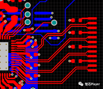
Figure 4 – Differential pair routing from IC to magnetics
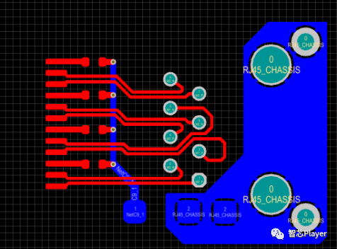
Figure 5 – Differential pair routing from magnetics to RJ45
RJ45 & Magnetics
- Connect RJ45 metal shield to chassis GND to reduce EMI.
- Use Bob Smith termination: 75 Ω + 1000 pF (3 kV rated) from center tap to chassis GND.
- Isolate chassis GND from circuit GND with a gap.
- Clear all planes under the high‑voltage barrier between magnetics and RJ45.
- For best ESD: use RJ45 without LEDs; use SMT contact type.
ETHRBIAS / ISET
- This is a high‑impedance, noise‑sensitive pin.
- Place the setting resistor very close to the pin.
- Keep traces short, isolated, with a direct, short return path to GND.
3. EMI Considerations
- Address EMC early in schematic and PCB design.
- Key emission sources: clocks, buses, repetitive signals.
- Key immunity risks: reset, interrupt, control lines.
- Use slower edge rates to reduce EMI.
- Multilayer boards have far better EMI performance.
- Do not embed traces in power/GND planes.
- Filter all I/O lines with high‑frequency filters.
- Isolate I/O sections properly.
4. ESD Considerations
- RJ45 must have a metal shield bonded to chassis GND at two points.
- Clear a 0.250‑inch high‑voltage barrier area between magnetics and RJ45.
- Route ESD currents away from sensitive circuits.
- Keep all signal traces as short as possible.
- Add ground guard traces for lines > 12 inches.
- Prevent ESD currents from entering digital GND (avoids ground bounce).
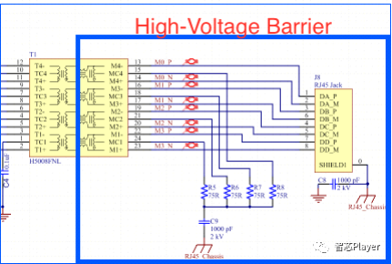
Figure 6 – High‑voltage barrier extending to the magnetics
About Maxipcb
Maxipcb empowers innovators to turn cutting-edge technologies into reality.
We offer one-stop solutions for design, simulation, testing, PCB manufacturing, component procurement and SMT assembly, enabling efficient development, rapid deployment and risk control across the full product lifecycle.Serving the world in communications, industrial automation, aerospace, automotive, semiconductor and beyond, we build a safer, more connected future together.


