Definition of High-Frequency PCB
High-frequency laminates are special circuit boards with high electromagnetic frequencies, used in high-frequency (frequency > 300 MHz or wavelength < 1 m) and microwave (frequency > 3 GHz or wavelength < 0.1 m) applications. They are manufactured using partial processes of conventional rigid circuit board manufacturing or special processing methods on microwave substrate copper-clad laminates. Generally, high-frequency PCBs can be defined as circuit boards operating at frequencies above 1 GHz.
With the rapid development of science and technology, more and more devices are designed for applications in the microwave band (> 1 GHz) and even the millimeter-wave band (> 77 GHz) (e.g., the popular automotive 77 GHz millimeter-wave antenna). This means that as frequencies increase, the requirements for circuit board substrates become increasingly stringent. For example, substrate materials must have excellent electrical properties, good chemical stability, and extremely low signal loss as the frequency of power signals increases. Therefore, the importance of high-frequency laminates has become prominent.
Classification of High-Frequency PCB Laminates
A. By Material
a. Organic materials: Phenolic resin, glass fiber/epoxy resin, Polyimide, BT/Epoxy, etc.
b. Inorganic materials: Aluminum, Copper-invar-copper, ceramic, etc., mainly used for their heat dissipation function
B. By Rigidity of Finished Products
a. Rigid PCB, b. Flexible PCB, c. Rigid-Flex PCB
C. By Structure
a. Single-sided board, b. Double-sided board, c. Multi-layer board
D. By Application
Communications/consumer electronics/military/computers/semiconductors/test boards...
Common High-Speed Laminates (Manufacturers) --- Welcome to reply with supplements
Domestic laminates offer high cost-effectiveness with performance comparable to imported products. Representative manufacturers include: Shengyi (Dongguan), Wangling (Taizhou), Taixing Microwave, Zhongying (Changzhou), Gongli Ceramic Boards, etc.
Foreign manufacturers:
- Rogers: RO4003, RO3003, RO4350, RO5880, etc. With the development of 5G millimeter-wave technology, Rogers has also launched a variety of low-loss circuit boards suitable for millimeter-wave applications.
- RO3000 Series: Ceramic-filled PTFE circuit materials, models include RO3003, RO3006, RO3010, RO3035 high-frequency laminates.
- RT6000 Series: Ceramic-filled PTFE circuit materials designed for electronic and microwave circuits requiring high dielectric constants. Models include RT6006 (dielectric constant 6.15) and RT6010 (dielectric constant 10.2).
- TMM Series: Composite materials based on ceramics, hydrocarbons, and thermosetting polymers. Models include TMM3, TMM4, TMM6, TMM10, TMM10i, TMM13i, etc.
- Taconic: TLX Series, TLY Series, etc.
- Panasonic: Megtron4, Megtron6, etc.
- Isola: FR408HR, IS620, IS680, etc.
- Nelco: N4000-13, N4000-13EPSI, etc.
- TUC: Tuc862, 872SLK, 883, 933, etc.
Of course, many other high-frequency laminates are not listed here. Among them, Arlon (acquired by Rogers) is also an established brand of RF and microwave board manufacturers.
Key Indicators for Selecting High-Frequency and High-Speed PCB Materials
When selecting substrates for high-frequency circuit PCBs, special attention should be paid to the variation characteristics of the material's DK (Dielectric Constant) at different frequencies. For requirements focusing on high-speed signal transmission or characteristic impedance control, the focus should be on DF (Dissipation Factor) and its performance under conditions of frequency, temperature, and humidity.
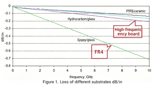
Conventional substrate materials exhibit significant variations in DK and DF values with changes in frequency, especially in the frequency range from 1 MHz to 1 GHz. For example, conventional epoxy resin-glass cloth-based substrate materials (conventional FR-4) have a DK value of 4.7 at 1 MHz, which changes to 4.19 at 1 GHz. Above 1 GHz, the change in DK value tends to flatten, showing a slight decreasing trend with increasing frequency (but with a small amplitude). For example, the DK value of conventional FR-4 is 4.15 at 10 GHz.
Substrate materials with high-speed and high-frequency characteristics show minimal changes in DK values with frequency, typically maintaining a variation within 0.02 from 1 MHz to 1 GHz. Their DK values show a slight downward trend at different frequencies from low to high.
The variation in the Dissipation Factor (DF) of conventional substrate materials due to frequency changes (especially in the high-frequency range) is greater than that of DK, and its variation trend is increasing. Therefore, when evaluating the high-frequency characteristics of a substrate material, the focus should be on its DF value variation. In terms of high-frequency variation characteristics, substrate materials with high-speed and high-frequency characteristics are significantly different from conventional substrate materials in two categories: one category shows very little change in DF value with frequency; the other category has a lower inherent DF value despite a similar variation amplitude to conventional substrate materials.
How to Select High-Frequency and High-Speed Laminates
The selection of PCB laminates must strike a balance between design requirements, mass producibility, and cost. In simple terms, design requirements include both electrical and structural reliability. This issue becomes particularly important when designing very high-speed PCB boards (frequencies above GHz). For example, the commonly used FR-4 material has a very high dielectric loss (Df) at several GHz frequencies and may not be suitable.
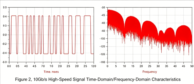
For example, a 10 Gb/s high-speed digital signal is a square wave, which can be regarded as a superposition of sinusoidal signals of different frequencies. Therefore, a 10 Gb/s signal contains many different frequency components: the 5 GHz fundamental signal, the 3rd harmonic 15 GHz, the 5th harmonic 25 GHz, the 7th harmonic 35 GHz, etc. Maintaining the integrity of digital signals and the steepness of their rising and falling edges is the same as achieving low-loss and low-distortion transmission in RF and microwave applications (where the high-frequency harmonic components of digital signals reach the microwave band). Therefore, in many aspects, the material selection requirements for high-speed digital circuit PCBs are similar to those for RF and microwave circuits.
In actual engineering practice, the selection of high-frequency laminates may seem simple, but it requires consideration of many factors. Through the introduction in this article, PCB design engineers or high-speed project managers can gain a certain understanding of the characteristics and selection of laminates, including their electrical, thermal, and reliability properties. By rationally using stack-up design, products with high reliability and good processability can be developed, achieving the optimal balance of various factors.
The main factors to consider when selecting appropriate laminates are described below:
-
Manufacturability:
Such as multiple lamination performance, temperature performance, CAF resistance/heat resistance, mechanical toughness (adhesion) (good reliability), and fire rating.
-
Various performance matching the product (electrical, performance stability, etc.):
Low loss, stable Dk/Df parameters, low dispersion, small variation coefficient with frequency and environmental conditions, tight tolerances on material thickness and resin content (good impedance control). For long traces, low-roughness copper foil should be considered. In addition, simulation is required in the early stage of high-speed circuit design, and simulation results are the reference standard for design. The "Xingsheng Technology-Agilent (High-Speed/RF) Joint Laboratory" has solved the industry challenge of inconsistent simulation and test results, conducted extensive closed-loop verification of simulation and actual testing, and achieved consistency between simulation and actual measurement through unique methods.
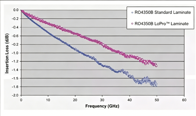
Figure 3. Measured loss comparison between 7.3mil standard RO4350B and low-roughness copper foil RO4350B LoPro laminates
-
Timely availability of materials:
Many high-frequency laminates have very long procurement cycles, even 2-3 months. Except for the conventional high-frequency laminate RO4350 which is in stock, most high-frequency boards require customer-specific orders. Therefore, it is necessary to communicate with manufacturers in advance and stock up early for high-frequency laminates.
-
Cost factor:
Depends on the price sensitivity of the product, whether it is consumer electronics, or communications, medical, industrial, military applications.
-
Applicability of laws and regulations:
Must comply with environmental regulations of different countries, meeting RoHS and halogen-free requirements.
Among the above factors, the operating speed of high-speed digital circuits is the main consideration for PCB selection. The higher the circuit speed, the smaller the Df value of the selected PCB should be. Medium and low loss circuit laminates are suitable for 10 Gb/s digital circuits; lower loss laminates are suitable for 25 Gb/s digital circuits; ultra-low loss laminates are suitable for faster high-speed digital circuits with speeds of 50 Gb/s or higher.
From the perspective of material Df:
- Laminates with Df between 0.01 and 0.005 are suitable for digital circuits up to 10 Gb/s;
- Laminates with Df between 0.005 and 0.003 are suitable for digital circuits up to 25 Gb/s;
- Laminates with Df not exceeding 0.0015 are suitable for 50 Gb/s and higher speed digital circuits.
Processing Methods
-
Cutting: Must be cut with the protective film retained to prevent scratches and indentations.
-
Drilling:
2.1 Use brand new drill bits (standard 130°), one board per stack is optimal, with a presser foot pressure of 40 psi.
2.2 Use aluminum sheet as the cover plate, then a 1 mm melamine backing plate, and clamp the PTFE board tightly.
2.3 Blow out dust in the holes with an air gun after drilling.
2.4 Use the most stable drilling machine. Drilling parameters: basically, the smaller the hole, the faster the drilling speed, the smaller the chip load, and the smaller the retraction speed.
-
Hole Treatment:
Plasma treatment or sodium-naphthalene activation treatment to facilitate hole metallization.
-
PTH (Plated Through Hole) Copper Plating:
4.1 After micro-etching (controlled at a micro-etching rate of 20 microinches), feed the board into the PTH line starting from the degreasing tank.
4.2 If necessary, perform a second PTH, feeding the board only from the expected tank.
-
Solder Mask:
5.1 Pretreatment: Use acid board cleaning, no mechanical brushing.
5.2 Bake the board after pretreatment (90°C, 30 min), then apply green solder mask and cure.
5.3 Bake in three stages: 80°C, 100°C, 150°C, 30 minutes each. If solder mask peeling is found on the substrate surface, rework can be done: wash off the green solder mask and re-perform activation treatment.
-
Routing:
Lay white paper on the circuit side of the PTFE board, and clamp it up and down with 1.0 mm thick etched copper-free FR-4 substrate boards or phenolic base plates。
The above summarizes how to select high-speed laminates and design considerations. In actual applications, specific analysis must be carried out according to specific cases.
About Maxipcb
Maxipcb enables advanced electronic innovation. We deliver one-stop solutions including circuit design, simulation, testing, PCB fabrication, component sourcing and SMT&PCBA assembly, to boost R&D efficiency, speed up mass production and control full-cycle risks. We serve global sectors like communication, industrial automation, aerospace, automotive and semiconductor, jointly forging a safer, connected intelligent future.


