RF antenna design and layout is one area that requires careful attention to detail, and it also provides some tips for mixed-signal designers. If you are new to high-frequency analog design, you can adopt the techniques provided in this article to ensure your RF design achieves excellent isolation and signal integrity.
RF antenna design and layout is one area that requires careful attention to detail, and it also provides some tips for mixed-signal designers. If you are new to high-frequency analog design, you can adopt the techniques provided in this article to ensure your RF design achieves excellent isolation and signal integrity.
Today, it is hard to think of a single consumer product that does not contain an antenna. Even my garage door opener can connect to a mobile phone via Bluetooth or Wi-Fi. Each time a new RF antenna is added to a PCB layout, it presents new challenges for RF designers—especially as analog design skills are once again playing a critical role. As various RF functions are integrated into new PCBs, how can designers ensure that signals within the system remain undisturbed and maintain signal integrity?
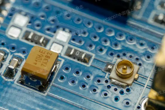
Figure 1. This SMA connector is coaxially connected to the RF antenna
Fortunately, there are simple design choices that can be made to ensure RF signals are not attenuated by surrounding digital components. These same design solutions also help prevent mutual interference between multiple analog signals. While many RF design factors must be considered when designing mixed-signal or full-RF systems, antenna design and layout are likely the two most critical elements. The following content will help you understand the essential knowledge in the field of PCB RF antenna design and how to ensure analog signal integrity.
Basic Key Points of RF Antenna Design
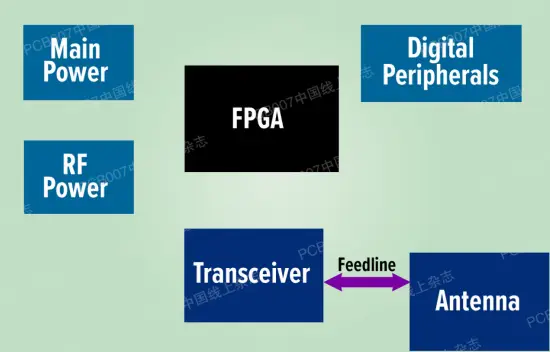
Figure 2. Gridded system layout on an RF PCB
- Floating Conductive Radiator: The element that emits radiation from the antenna.
- Reference: The antenna reference plane or element that helps define the directivity of the structure in each antenna mode.
- Feedline: The feedline transmits the input signal from the RF components to the radiating antenna element.
- Impedance-Matching Network: Antennas typically have an impedance of approximately 10 ohms, so they need to be impedance-matched to the feedline to prevent reflections and ensure maximum transmitted power at the desired carrier frequency and bandwidth.
A vast number of standard antenna designs have been researched. Many reference designs can be found online and copied into PCB layouts. Design formulas for many standard antenna structures can also be found in microwave engineering textbooks.
If you wish to use COTS RF antennas, many low-cost designs are available on the market. Regardless of which RF antenna you choose, it must be carefully placed in the PCB layout to prevent interference between different sections.
RF Antenna Layout Techniques
Once the antenna is designed, it is time to determine where it should be placed on the PCB. RF designers should take advice from mixed-signal designers (most RF PCBs are in fact mixed-signal PCBs) to prevent interference between multiple sections of the RF front-end, back-end, and digital sections.
- Effective Radiation: The goal is to ensure that radiation from the antenna elements travels away from the PCB and is not received by other structures in the PCB layout.
- Isolation: Similarly, mutual interference between multiple sections of the PCB layout must be avoided.
- Electromagnetic Compatibility (EMC): It is necessary to ensure that the PCB layout does not receive signals emitted by other devices (which may transmit across a wide frequency range).
In practical PCB design, most design objectives compete with one another (in terms of priority), but two key points can help balance these objectives.
1. Separate Circuit Blocks in the PCB Layout
This is a fundamental topic in mixed-signal PCB design, and it applies equally to RF antenna layout. The antenna’s position on the PCB must be separated from other circuit blocks. Generally, it is best to place the antenna section near the edge of the PCB, away from other analog components. This confines strong radiation to a specific location on the PCB and ensures minimal interference between different sections of the board.
The challenge of gridded layout is to ensure that return paths in different areas do not interfere with one another; otherwise, noise coupling and crosstalk will occur. Field solvers integrated into advanced PCB design tools can help identify return path deviations during PCB layout construction. For high-frequency designs, a continuous ground plane structure ensures consistent return paths.
2. Isolate the Antenna Section
Modern mobile phones and cellular devices have become the gold standard for RF isolation technology due to their innovative isolation structures. Simply put, isolation involves placing shielding around RF-sensitive elements on the PCB to block wave propagation between transmitters and receivers. The following solutions can be used in the RF antenna section to isolate components, feedlines, and antennas from one another or from external noise sources.
Isolation structures are typically placed between RF elements to prevent noise coupling or power exchange between them. Determining which isolation structure to use to preserve the signal integrity of RF antennas is a complex, well-researched design problem. If you are not an expert in elliptic integral mathematics, you will need to rely on electromagnetic (EM) field solvers to determine the impact of these structures on feedline and RF antenna impedance, as well as the isolation strength of these structures.
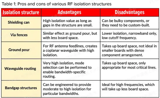
Figure 3. Advantages and disadvantages of various RF isolation structures
If an EM field solver is available, near-field and far-field simulations can be used to identify areas of strong radiation in the PCB layout. Once the locations of these areas and the frequencies they emit are determined, it is easier to decide which type of isolation method to use. It is preferable to use a Finite Element Method (FEM) solver directly, rather than converting FDTD results using Fourier transforms.
Although RF antenna design and layout require extra attention to detail, the effort pays off by ensuring excellent isolation and signal integrity in RF designs.
Key Takeaways
- RF antennas come in various forms, from on-chip planar antennas integrated into ICs to copper antennas printed directly on PCBs.
- When designing a PCB layout with one or more antennas, it is necessary to ensure effective isolation between different circuit modules on the PCB.
- When designing RF antennas, CAD tools should be used to assist in designing isolation structures, transition structures, and even printed antennas on the PCB.
About Maxipcb
Maxipcb empowers innovators to turn cutting-edge technologies into reality.
We offer one-stop solutions for design, simulation, testing, PCB manufacturing, component procurement and SMT assembly, enabling efficient development, rapid deployment and risk control across the full product lifecycle.Serving the world in communications, industrial automation, aerospace, automotive, semiconductor and beyond, we build a safer, more connected future together.


 Figure 3. Advantages and disadvantages of various RF isolation structures