Impedance Design: A Factor Affecting Radiated Emission of High-Speed Differential Signals
1. In-Depth Analysis of Impedance's Impact on Radiated Emission of High-Speed Differential Signals
Ideally, perfect impedance matching between the source impedance, cable impedance, and sink impedance enables lossless signal transmission. In practice, however, complete impedance matching is unattainable, mainly due to impedance discontinuities at connectors, poor impedance control of cables, inadequate impedance management in PCB routing, and inherent impedance design of devices.
High-speed differential signal specifications clearly define a general impedance design requirement of 100±15% to ensure signal transmission quality. From an EMC perspective, impedance discontinuities and mismatches cause signal reflection, leading to overshoot, ringing, and standing waves. These issues further result in radiated emission of the signal's fundamental frequency and high-order harmonics.
The Relationship Between Impedance and Radiated Emission of High-Speed Differential Signals
Meeting the characteristic impedance standard of 100±15Ω does not guarantee the smooth passing of radiated emission tests for high-speed differential signals. Transient impedance has a more significant impact on test results than characteristic impedance. When the 100±15Ω impedance limit is satisfied, a flatter transient impedance (the smaller the impedance variation range, the better) means the signal experiences minimal transient impedance changes, leading to the lowest possible radiated energy to the external space.
Impedance matching is a necessary but not sufficient condition for passing the radiated emission test of high-speed differential signals—impedance mismatch will definitely adversely affect the test results. Setting aside source and cable impedance, this article focuses on the sink-end impedance.
Practical Factors Affecting Impedance
Impedance is influenced by factors including: trace width and spacing, copper thickness, dielectric material and thickness, distance from the reference plane, and the width and thickness of component pad pins. Strict control of these factors during impedance design, combined with rigorous manufacturing process control, is essential for achieving PCB routing with precise impedance.
2. Principles for Impedance Design Control
With numerous factors affecting impedance, mastering impedance design control is a compulsory skill for EMC engineers. As the width and thickness of component pads/pins are among the impedance-influencing factors, minimizing the number of components in high-speed differential signal links is recommended to strictly control impedance discontinuity points and achieve a flat impedance test curve.
In addition, impedance optimization can be implemented through PCB design at the connector pins of interconnection interfaces, pad pins of BGA chips, and pads of ESD protection devices—despite their standardized device design.
Trace width and spacing, copper thickness, and dielectric material/thickness for differential signals must be strictly controlled during PCB design and measured during manufacturing. In multi-layer board design, cross-partitioning not only impairs the integrity of the signal return path but also distorts signal impedance; thus, the integrity of the reference ground plane must be a key focus in PCB design.
Impedance at the connection points is often low due to chip design flaws or poor terminal design of high-speed differential signals—series matching resistors should be added in such cases. If the impedance at the connection points is excessively high, adjust the pad width and pin routing width to calibrate the impedance.
Most interconnections between high-speed differential signal devices rely on cables, whose impedance design and control are among the most critical factors for impedance matching. In practice, the varying quality of cable manufacturers makes cables a bottleneck for passing radiated emission tests. FFC cables are commonly used for high-speed differential signal interconnection, with mature impedance control technology in the industry—the impact of bending points on impedance discontinuity is the main concern.
3. Case Studies of PCB Impedance Design
Case 1: Optimizing Impedance by Modifying Device PCB Packages
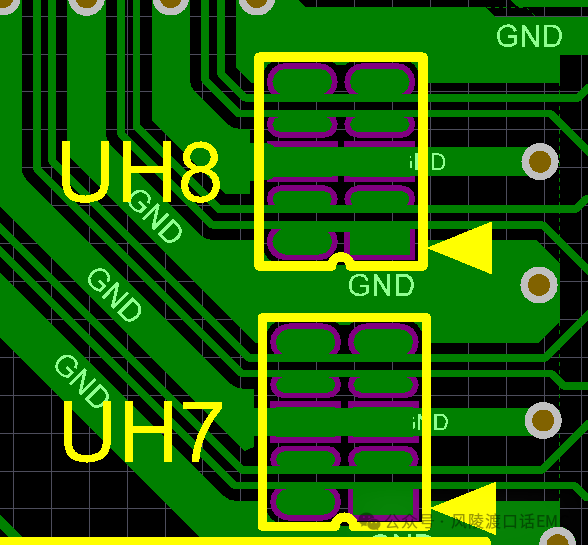
Differential signal impedance design before PCB Layout modification
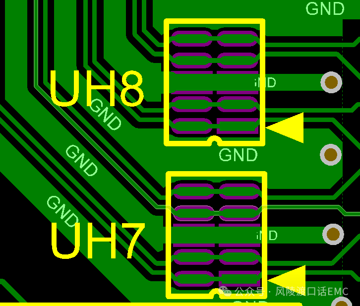
Differential signal impedance design after PCB Layout modification
Case Analysis:
Component pad pins are the primary locations of severe impedance discontinuity. In actual PCB design, impedance optimization can be achieved by modifying the size of component pad pins. For multi-layer boards,
clearance processing of the reference layer under the device is required to compensate for the impact of reference layer spacing, ensuring the impedance design meets standard requirements.
Case 2: Optimizing Impedance by Controlling Trace Width Variation
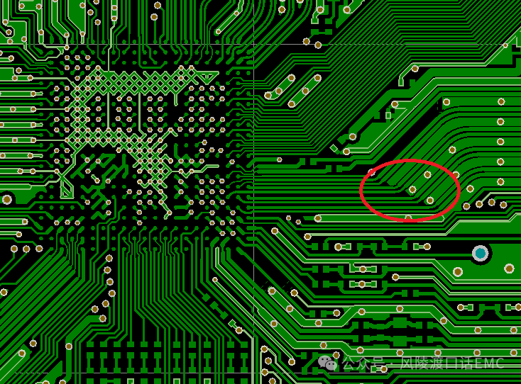 Differential signal impedance design before PCB Layout modification
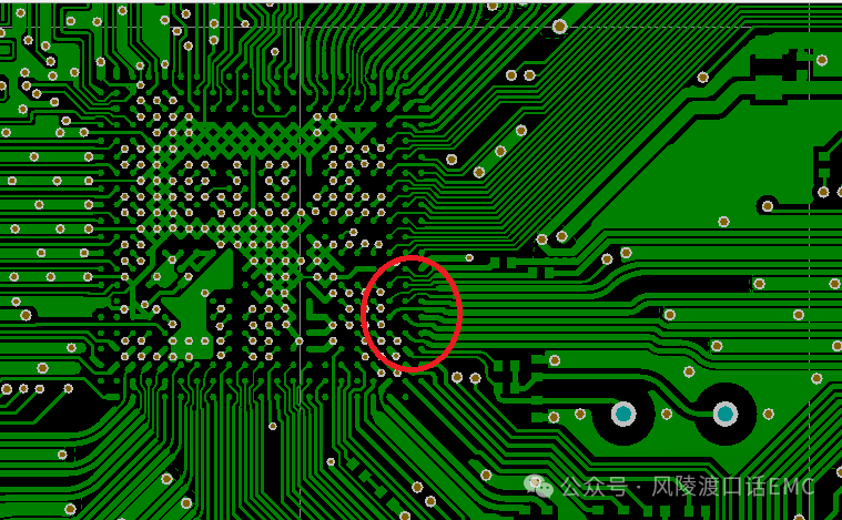 Differential signal impedance design after PCB Layout modification
Case Analysis:
Impedance changes with the variation of PCB trace width, and the severity of impedance change is proportional to the degree of trace width variation. The optimal solution to impedance discontinuity caused by abrupt trace width changes is to keep the trace width constant—an unattainable goal in actual PCB design. The alternative is to use
tapered traces to mitigate the issue.
Case 3: The Impact of Dielectric Thickness on Impedance
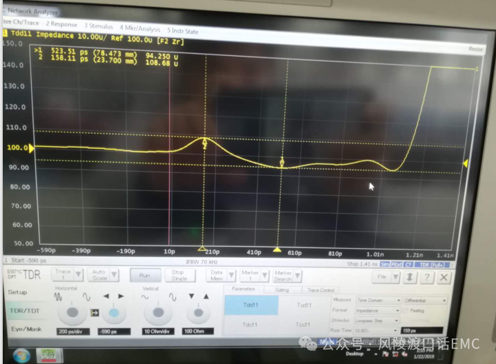 Impedance of high-speed differential signal traces before removing the sticker (tested by Network Analyzer/TDR)
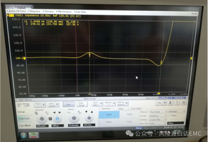 Impedance of high-speed differential signal traces after removing the sticker (tested by Network Analyzer/TDR)
Case Analysis:
Dielectric material and thickness are crucial factors affecting impedance. Since high-speed differential signal traces are usually flat with few components, PCB designers often place board information stickers and model silkscreens on these traces. Unknowingly, this practice causes
impedance discontinuity of high-speed differential signals, leading to signal reflection and radiated emission issues.
About Maxipcb
Maxipcb empowers innovators to turn cutting-edge technologies into reality.
We offer one-stop solutions for design, simulation, testing, PCB manufacturing, component procurement and SMT assembly, enabling efficient development, rapid deployment and risk control across the full product lifecycle.Serving the world in communications, industrial automation, aerospace, automotive, semiconductor and beyond, we build a safer, more connected future together.


 Differential signal impedance design before PCB Layout modification
 Differential signal impedance design before PCB Layout modification
 Differential signal impedance design after PCB Layout modification
 Impedance of high-speed differential signal traces before removing the sticker (tested by Network Analyzer/TDR)
 Impedance of high-speed differential signal traces after removing the sticker (tested by Network Analyzer/TDR)