BGA stands for Ball Grid Array, a packaging technology for integrated circuits using organic substrates. It is widely used for permanent mounting of microprocessors and provides far more interconnection pins than dual-in-line or flat packages. BGA utilizes the entire bottom surface of the package (not just the edges), and the internal traces connecting the die to the solder balls are shorter, delivering better high‑speed performance.
What is BGA?
BGA stands for Ball Grid Array, a packaging technology for integrated circuits using organic substrates. It is widely used for permanent mounting of microprocessors and provides far more interconnection pins than dual-in-line or flat packages. BGA utilizes the entire bottom surface of the package (not just the edges), and the internal traces connecting the die to the solder balls are shorter, delivering better high‑speed performance.
Key Features of BGA:
- Reduced package size
- Higher functionality with increased pin count
- Self‑alignment during reflow, easy soldering
- High reliability
- Good electrical performance and low overall cost
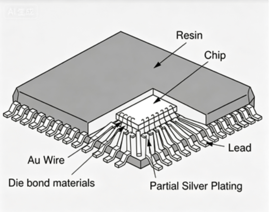
BGA internal structure diagram
(Resin, Chip, Lead, Au Wire, Die bond materials, Partial Silver Plating)
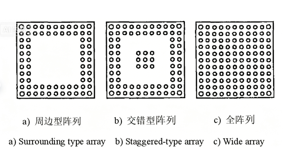
BGA array types:a) Perimeter array, b) Staggered array, c) Full array
PCBs with BGAs usually contain many small vias. Typical finished via diameters under BGAs are 8–12 mil. For a 31.5‑mil BGA pitch, the distance from surface mount pads to vias is generally no less than 10.5 mil. Vias under BGAs require plugging, and BGA pads must not be covered with solder mask or drilled.
Most BGA packages use flip‑chip interconnection instead of traditional wire bonding. Flip‑chip design allows direct attachment of heat sinks for improved thermal dissipation.
BGA Packaging Process Flow
Wafer bumping → Wafer dicing → Flip‑chip mounting & reflow → Underfill → Thermal grease & sealant dispensing → Lid attachment → Solder ball assembly → Reflow → Marking → Singulation → Final inspection → Testing → Encapsulation
Flip‑chip bonding breaks through the pitch limit of wire‑bond pads, simplifies power/ground distribution, and supports better signaling for high‑frequency, high‑power devices. BGA soldering requires precise control, typically using computer‑controlled automatic laser ball placement + reflow.
Common Bumping Methods
Three mainstream methods for creating solder bumps:
- Electroplating – complex, high cost, long cycle, environmental impact
- Solder paste printing – difficult to control height; not suitable for bumps < 200 μm
- Laser solder ball placement – stable, clean, high precision, ideal for micro‑BGA
Advantages of Laser Solder Ball Placement
-
High‑efficiency, stable heat source
Uses fiber laser with high electro‑optical conversion efficiency and stable energy output.
-
Wide compatibility & high precision
Supports solder balls of
0.07 mm–0.20 mm (SAC, Sn‑Bi‑Ag, etc.). CCD vision positioning ensures accurate placement.
-
Non‑contact, high speed
Up to
3–5 balls/second. Stable solder volume, excellent consistency, easy automation.
-
Low thermal impact
No global heating; minimal thermal effect on surrounding wafer materials and pre‑existing bumps.
-
Clean, flux‑free process
Solder balls contain no flux, eliminating post‑process cleaning. Zero pollution, fully compliant with green manufacturing.
About Maxipcb
Maxipcb empowers innovators to turn cutting-edge technologies into reality.
We offer one-stop solutions for design, simulation, testing, PCB manufacturing, component procurement and SMT assembly, enabling efficient development, rapid deployment and risk control across the full product lifecycle.Serving the world in communications, industrial automation, aerospace, automotive, semiconductor and beyond, we build a safer, more connected future together.


