The integration of electronic systems is mainly divided into three levels: on-chip integration, in-package integration, and PCB board-level integration
Levels of Integration
The integration of electronic systems is mainly divided into three levels:
on-chip integration,
in-package integration, and
PCB board-level integration, as shown in the figure below:
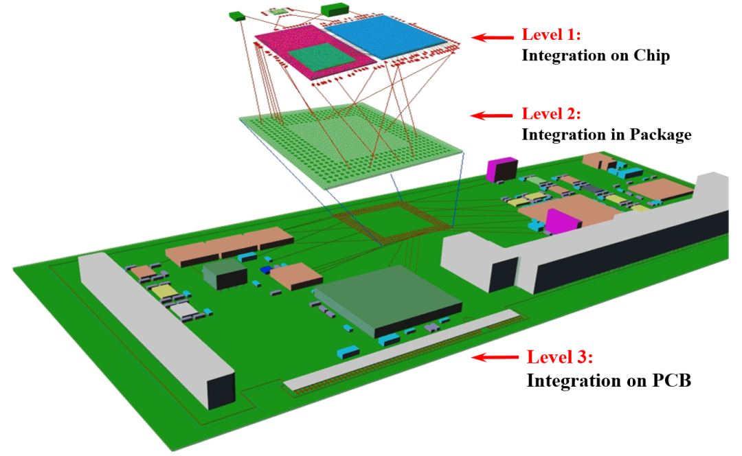 Level 1
: Integration on Chip
Level 2: Integration in Package
Level 3: Integration on PCB
The basic units of in-package integration are bare chips or chiplets completed in the previous step, which we call Functional Units. These functional units are integrated within the package to form a SiP (System in Package).
On-Chip Integration
From a minimalist perspective, we need to understand three types of materials and three types of processes.
Three Core Materials: Conductors, Semiconductors, Insulators
Although a wide variety of materials are used on chips—modern integrated circuits utilize nearly all elements of the periodic table—all materials can be categorized into three groups: conductors, semiconductors, and insulators.
- Conductors are responsible for electron transmission.
- Insulators isolate electrons.
- Semiconductors are the most critical, as their properties are switchable: they can act as conductors (ON state) to allow electron flow, or as insulators (OFF state) to block it. This switch is controllable by designing special structures and applying electric current or voltage.
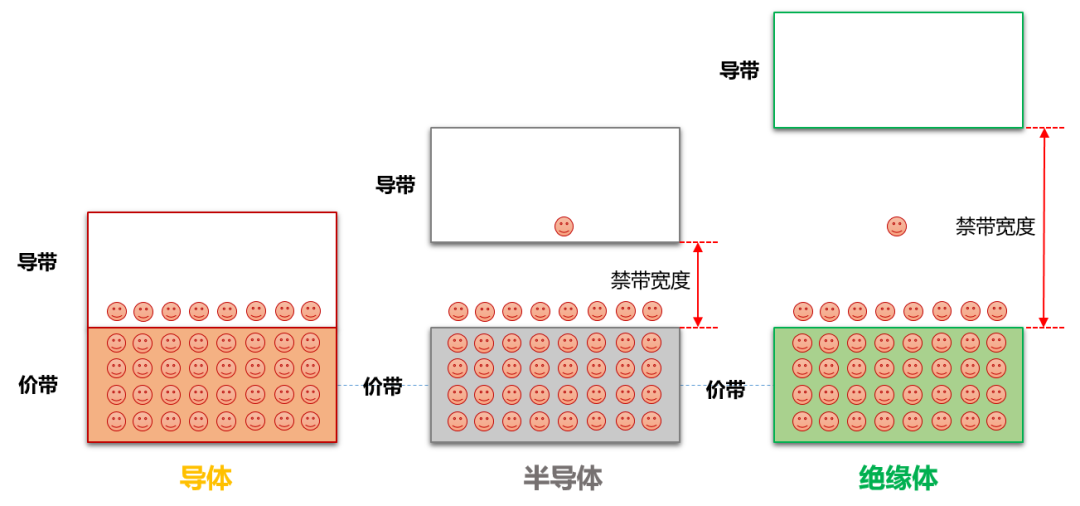 Conduction Band | Band Gap | Valence Band
Conductor • Semiconductor • Insulator
Conduction Band | Band Gap | Valence Band
Conductor • Semiconductor • InsulatorThree Core Processes: Additive, Subtractive, Pattern Transfer
- Additive processes: Essentially adding materials to a substrate. Examples include ion implantation, sputtering, Chemical Vapor Deposition (CVD), and Physical Vapor Deposition (PVD).
- Subtractive processes: Essentially removing materials from a substrate. Examples include etching, Chemical Mechanical Polishing (CMP), and wafer planarization.
- Pattern transfer: The most numerous and challenging of the three, as nearly all additive and subtractive processes are based on it. It involves transferring designed patterns onto a wafer, and relies on photomasks, lithography, and photoresists.
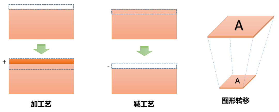 Additive Process • Subtractive Process • Pattern Transfer
The final product of on-chip integration is a wafer. When a wafer is diced, it forms chips or chiplets, which serve as the foundation for the next level of integration.
In-Package Integration
In-package integration does not utilize the characteristics of semiconductors, so its materials are mainly divided into two categories: conductors and insulators. The primary goal of integration is to electrically interconnect the chips or chiplets from on-chip integration within the package to form a
microsystem.
The end result of in-package integration is functional units represented by SiP and advanced packaging—these are what we call microsystems.
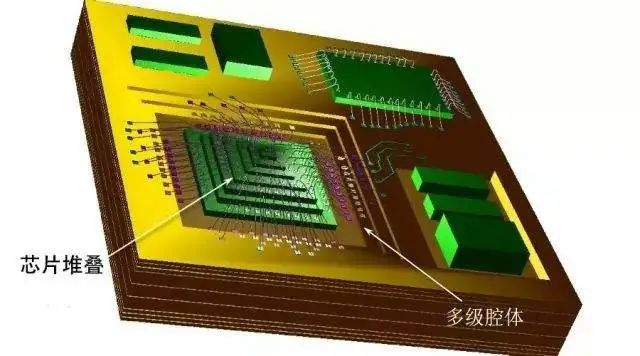 Chip Stacking • Multi-Level Cavity
PCB Board-Level Integration
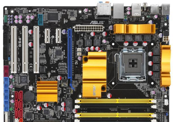
Today, PCBs almost universally feature double-sided component mounting, and board layers can reach dozens in number. High-Density Interconnect (HDI) boards, rigid-flex boards, microwave circuit boards, and embedded device boards are all widely used.
Like in-package integration, PCB-level integration does not use semiconductor characteristics, so its materials are also mainly conductors and insulators.
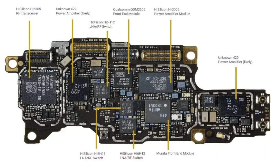
 HiSilicon Hi6365 Unknown 429 RF Transceiver
Qualcomm QDM2305 HiSilicon Hi6D05 Front-End Module Power Amplifier Module
Power Amplifier (likely)
HiSilicon Hi6H12 LNA/RF Switch
Unknown 429
HD99E1936 GFCV100
13-22 1936-TW 06
6365 429 92142 D23193 GV Hi6D05
g2142 180351 67 ehHTA 446
HiSilicon Hi6H11 HiSilicon Hi6H12 Murata Front-End Module
LNA/RF Switch LNA/RF Switch
HiSilicon Hi6365 Unknown 429 RF Transceiver
Qualcomm QDM2305 HiSilicon Hi6D05 Front-End Module Power Amplifier Module
Power Amplifier (likely)
HiSilicon Hi6H12 LNA/RF Switch
Unknown 429
HD99E1936 GFCV100
13-22 1936-TW 06
6365 429 92142 D23193 GV Hi6D05
g2142 180351 67 ehHTA 446
HiSilicon Hi6H11 HiSilicon Hi6H12 Murata Front-End Module
LNA/RF Switch LNA/RF SwitchStages of Integration
Stages of On-Chip Integration
On-chip integration is primarily divided into two core stages: device fabrication (also known as Front-End of Line, FEOL) and metal interconnection (also known as Back-End of Line, BEOL).
Device Fabrication (FEOL)
Device fabrication involves manufacturing functional "cells" such as transistors, resistors, capacitors, and diodes on a monocrystalline silicon wafer through process steps including lithography, etching, ion implantation, sputtering, CVD, PVD, CMP, and wafer planarization.
Current 5nm process technology can fabricate more than
100 million transistors per square millimeter.
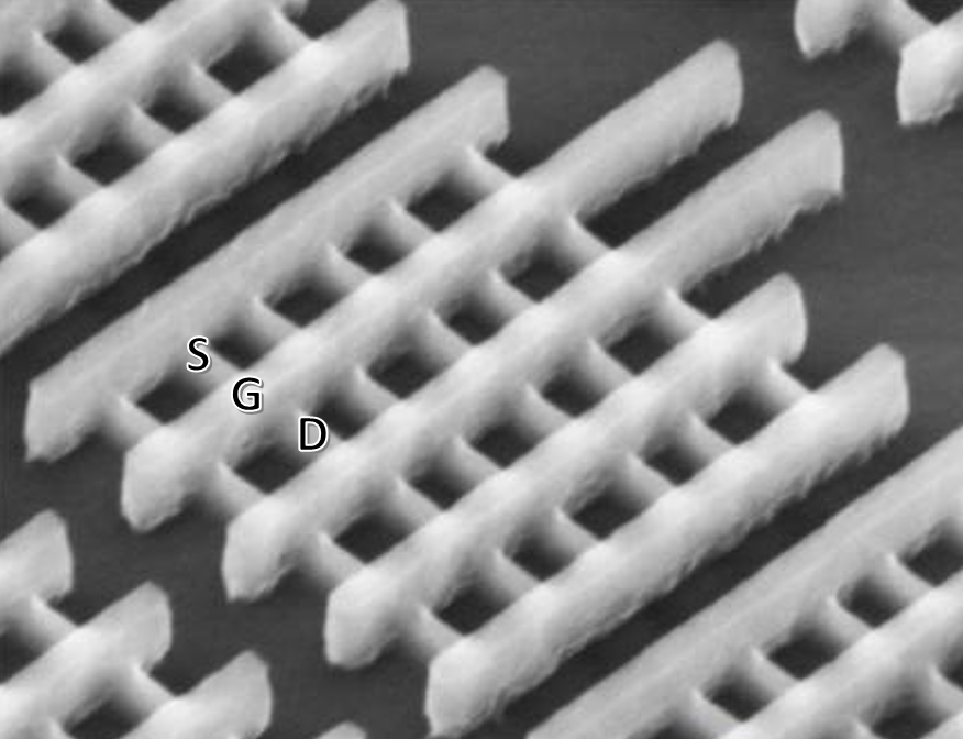 Micrograph of a FinFET transistor (the tall white beam is the Gate G; the short beam is the Fin, with a width approximately 0.67 times that of the gate; the Source S and Drain D are on either side of the gate).
Metal Interconnection (BEOL)
After the transistor layer is fabricated, contact vias are made with metals such as tungsten to connect the transistors to the first metal wiring layer. Electrical interconnection is then achieved through multi-layer metal wiring and vias.
Early chips used aluminum wiring, while modern chips mostly use
copper wiring.
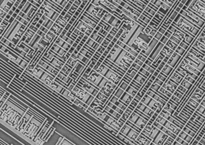 Micrograph of metal interconnections on a chip, showing a multi-layer wiring structure (current processes support more than 10 metal wiring layers).
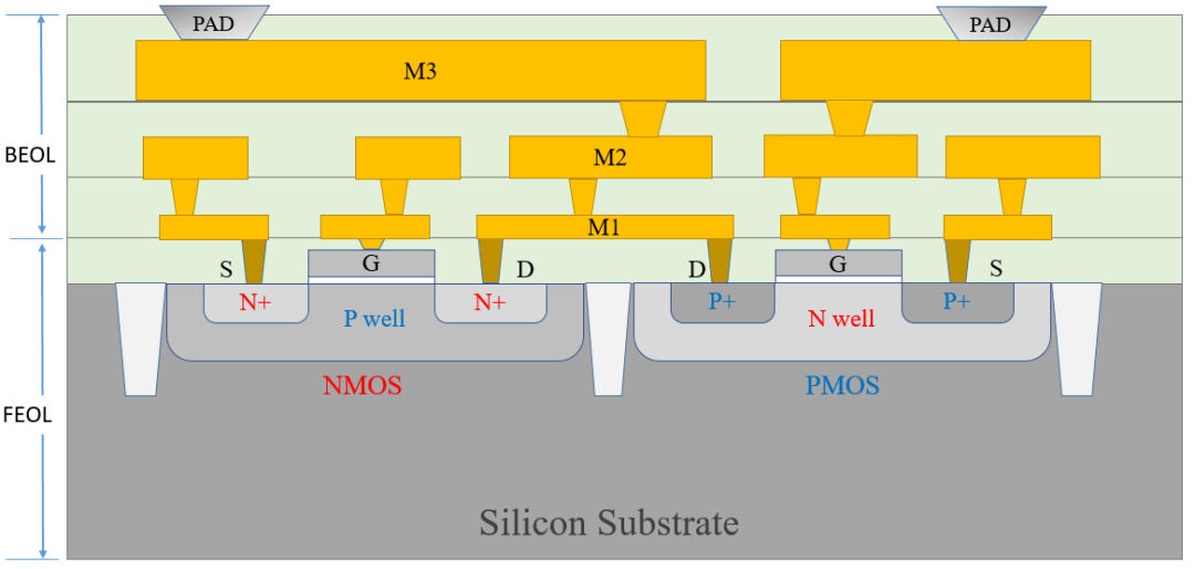 Schematic diagram of FEOL and BEOL structures: Transistors are first fabricated on a silicon substrate, then connected via metal interconnections and led out to the chip's PADs.
PAD PAD | M3 | BEOL M2 | M1 | S D D | N+ P well N+ P+ N well | NMOS PMOS | FEOL Silicon Substrate
Schematic diagram of FEOL and BEOL structures: Transistors are first fabricated on a silicon substrate, then connected via metal interconnections and led out to the chip's PADs.
PAD PAD | M3 | BEOL M2 | M1 | S D D | N+ P well N+ P+ N well | NMOS PMOS | FEOL Silicon SubstrateStages of In-Package Integration
The traditional approach is to connect the chip's PADs to a package substrate or lead frame using bond wires, which are then connected to external pins. Packaging forms are classified by pin arrangement, including BGA, CGA, QFP, LCC, SOP, DIP, and others.
 PAD | M3 | BAD | NMOS | Silicon Substrate
To increase the functional density within a package, more functional units need to be integrated—and traditional wire bonding can no longer meet the demand. This has led to the development of a variety of advanced packaging technologies, with the most typical ones introduced below:
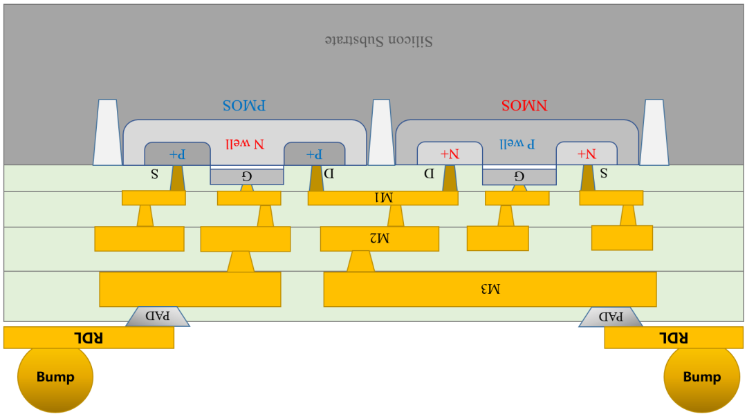
RDL and TSV Fabrication on Chips
Redistribution Layers (RDL) are fabricated on the chip surface to reroute PADs to more spacious positions and form bumps—this is referred to as
XY-plane extension.
The chip can then be directly mounted on a substrate via these bumps, a process known as
Flip Chip (the name is self-explanatory from the structure).
 Sis | PMOS NMOS | + Nwell +P +N P el +N | S G D D G S | MI | M2 | M3 | PAD PAD | RDL RDL | Bump Bump
Flip chips cannot be stacked, making Z-axis extension impossible. This led to the invention of
Through Silicon Via (TSV) technology—vias that penetrate the entire chip body.
TSV presents many process challenges, with
via position selection and
aperture miniaturization being the most critical to solve.
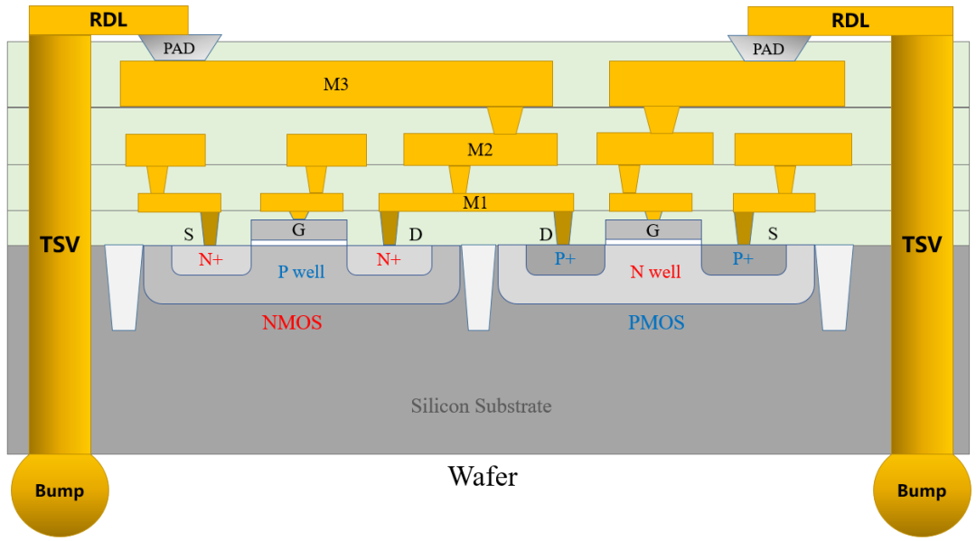 Schematic diagram of TSV on a chip: TSV connects the top and bottom surfaces of the chip with metal conductors, enabling chip stacking.
Bump | RDL RDL | PAD PAD | M3 | M2 | M1 | TSV G N+ D D P+ TSV | NMOS PMOS | Silicon Substrate | Wafer | Bump
Schematic diagram of TSV on a chip: TSV connects the top and bottom surfaces of the chip with metal conductors, enabling chip stacking.
Bump | RDL RDL | PAD PAD | M3 | M2 | M1 | TSV G N+ D D P+ TSV | NMOS PMOS | Silicon Substrate | Wafer | BumpRDL and TSV Fabrication on Interposers
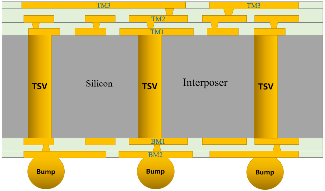 TM3 TM3 | TM2 | TM1 | TSV Silicon TSV Interposer TSV | BM1 | BM2 | Bump Bump Bump
Interconnect Line Fabrication on Substrates
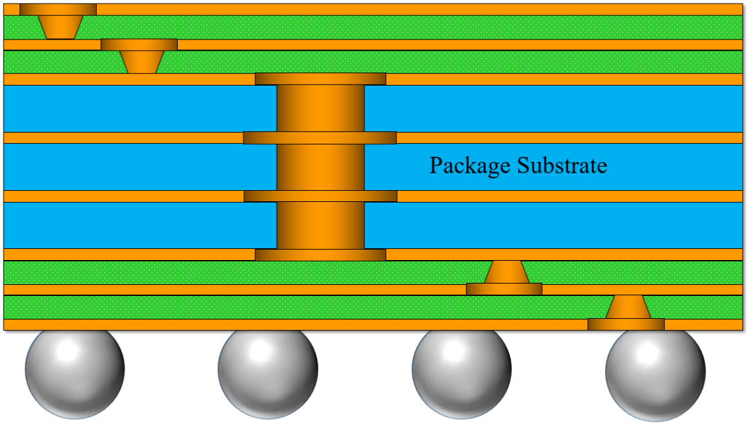 Package Substrate
Package substrates typically mount devices on the top and connect to PCBs via BGA on the bottom.
Package Substrate
Package substrates typically mount devices on the top and connect to PCBs via BGA on the bottom.Device Assembly and Packaging
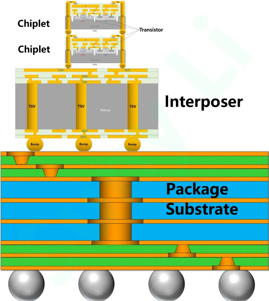 Chiplet | Transistor | Chiplet | TSV TSV Silicon TSV | BMI | BM2 | Bump Bump Bump | Interposer | M | Package Substrate
Stages of PCB Board-Level Integration
After in-package integration, the component size is still too small for most electronic products. Additionally, some discrete components (e.g., large capacitors, transformers) cannot be integrated into chip packages. For these reasons, PCBs remain an indispensable part of electronic products.
PCB Interconnect Line Fabrication
PCB manufacturing processes are similar to those of organic substrates, but PCBs have lower wiring density and a relatively simpler structure.
PCBs mostly use
through-hole structures—while high-density HDI boards now use blind and buried vias, through-holes are widely adopted due to their simple structure and low cost.
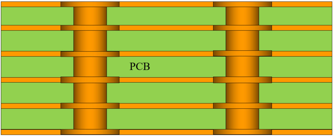 Schematic of a 6-layer through-hole PCB: PCBs fix components and achieve their electrical interconnection.
Component Assembly on PCBs
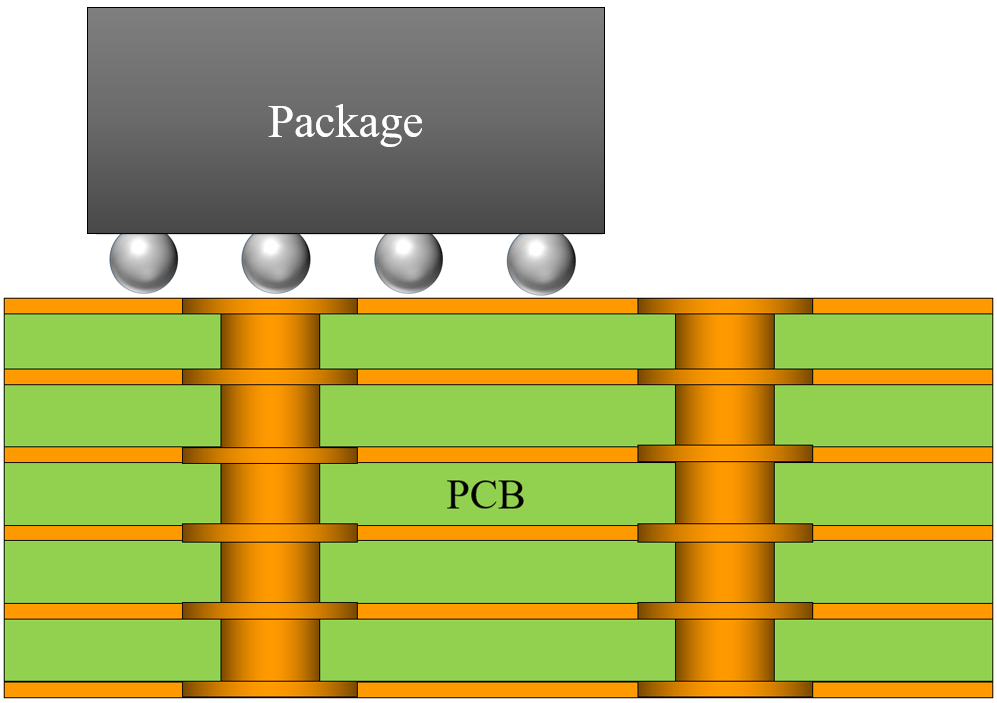 Package | PCB
Full Integration Diagram from Transistor to PCB
Below is a complete diagram of integration from transistors to PCBs:
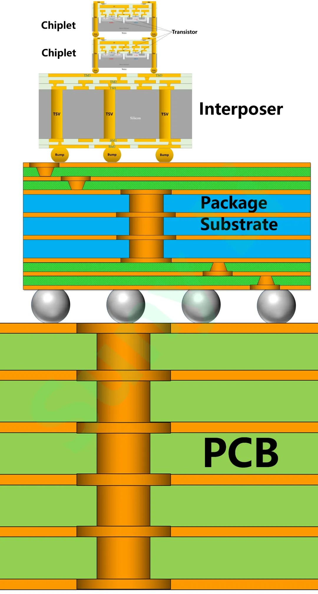 Chiplet Chiplet | TSV | TSV | Sil | Transistor | Interposer Package Substrate | PCB
Integration Process Summary:
Transistors (NMOS/PMOS) are fabricated on a silicon substrate → connected to on-chip metal wiring via contact vias → connected to chip PADs → routed to 3D TSV via RDL → connected to RDL and 2.5D TSV on a silicon interposer via μBump → connected to the package substrate via bumps → connected to BGA via interconnect lines and vias on the package substrate → finally connected to wiring and vias on the PCB.
About Maxipcb
Maxipcb empowers innovators to turn cutting-edge technologies into reality.
We offer one-stop solutions for design, simulation, testing, PCB manufacturing, component procurement and SMT assembly, enabling efficient development, rapid deployment and risk control across the full product lifecycle.Serving the world in communications, industrial automation, aerospace, automotive, semiconductor and beyond, we build a safer, more connected future together.

 Level 1: Integration on Chip
Level 2: Integration in Package
Level 3: Integration on PCB
Level 1: Integration on Chip
Level 2: Integration in Package
Level 3: Integration on PCB Conduction Band | Band Gap | Valence Band
Conductor • Semiconductor • Insulator
Conduction Band | Band Gap | Valence Band
Conductor • Semiconductor • Insulator Additive Process • Subtractive Process • Pattern Transfer
 Chip Stacking • Multi-Level Cavity
 HiSilicon Hi6365 Unknown 429 RF Transceiver
Qualcomm QDM2305 HiSilicon Hi6D05 Front-End Module Power Amplifier Module
Power Amplifier (likely)
HiSilicon Hi6H12 LNA/RF Switch
Unknown 429
HD99E1936 GFCV100
13-22 1936-TW 06
6365 429 92142 D23193 GV Hi6D05
g2142 180351 67 ehHTA 446
HiSilicon Hi6H11 HiSilicon Hi6H12 Murata Front-End Module
LNA/RF Switch LNA/RF Switch
HiSilicon Hi6365 Unknown 429 RF Transceiver
Qualcomm QDM2305 HiSilicon Hi6D05 Front-End Module Power Amplifier Module
Power Amplifier (likely)
HiSilicon Hi6H12 LNA/RF Switch
Unknown 429
HD99E1936 GFCV100
13-22 1936-TW 06
6365 429 92142 D23193 GV Hi6D05
g2142 180351 67 ehHTA 446
HiSilicon Hi6H11 HiSilicon Hi6H12 Murata Front-End Module
LNA/RF Switch LNA/RF Switch Micrograph of a FinFET transistor (the tall white beam is the Gate G; the short beam is the Fin, with a width approximately 0.67 times that of the gate; the Source S and Drain D are on either side of the gate).
 Micrograph of metal interconnections on a chip, showing a multi-layer wiring structure (current processes support more than 10 metal wiring layers).
 Schematic diagram of FEOL and BEOL structures: Transistors are first fabricated on a silicon substrate, then connected via metal interconnections and led out to the chip's PADs.
PAD PAD | M3 | BEOL M2 | M1 | S D D | N+ P well N+ P+ N well | NMOS PMOS | FEOL Silicon Substrate
Schematic diagram of FEOL and BEOL structures: Transistors are first fabricated on a silicon substrate, then connected via metal interconnections and led out to the chip's PADs.
PAD PAD | M3 | BEOL M2 | M1 | S D D | N+ P well N+ P+ N well | NMOS PMOS | FEOL Silicon Substrate PAD | M3 | BAD | NMOS | Silicon Substrate
 Sis | PMOS NMOS | + Nwell +P +N P el +N | S G D D G S | MI | M2 | M3 | PAD PAD | RDL RDL | Bump Bump
 Schematic diagram of TSV on a chip: TSV connects the top and bottom surfaces of the chip with metal conductors, enabling chip stacking.
Bump | RDL RDL | PAD PAD | M3 | M2 | M1 | TSV G N+ D D P+ TSV | NMOS PMOS | Silicon Substrate | Wafer | Bump
Schematic diagram of TSV on a chip: TSV connects the top and bottom surfaces of the chip with metal conductors, enabling chip stacking.
Bump | RDL RDL | PAD PAD | M3 | M2 | M1 | TSV G N+ D D P+ TSV | NMOS PMOS | Silicon Substrate | Wafer | Bump TM3 TM3 | TM2 | TM1 | TSV Silicon TSV Interposer TSV | BM1 | BM2 | Bump Bump Bump
 Package Substrate
Package substrates typically mount devices on the top and connect to PCBs via BGA on the bottom.
Package Substrate
Package substrates typically mount devices on the top and connect to PCBs via BGA on the bottom. Chiplet | Transistor | Chiplet | TSV TSV Silicon TSV | BMI | BM2 | Bump Bump Bump | Interposer | M | Package Substrate
 Schematic of a 6-layer through-hole PCB: PCBs fix components and achieve their electrical interconnection.
 Package | PCB
 Chiplet Chiplet | TSV | TSV | Sil | Transistor | Interposer Package Substrate | PCB