In integrated circuit application design, PCB layout design is required after the schematic design of the project is completed. PCB design is a crucial link, and the quality of the design results directly affects the functions of the entire design.
In integrated circuit application design, PCB layout design is required after the schematic design of the project is completed. PCB design is a crucial link, and the quality of the design results directly affects the functions of the entire design.
Therefore, reasonable and efficient PCB layout is a critical step for the successful debugging of chip circuit design. This article briefly introduces the key points of PCB layout design.
Key Points of PCB Layout Design
Component Package Selection
Resistor Selection: The withstand voltage, maximum power dissipation, and temperature of the selected resistor must not exceed the operating range.
| Resistor Package |
0402 |
0603 |
0805 |
1206 |
| Rated Power @70°C (mW) |
63 |
100 |
125 |
250 |
| Maximum Operating Voltage (V) |
50 |
50 |
150 |
200 |
Capacitor Selection: The withstand voltage and maximum effective current of the selected capacitor shall also be considered.
| Capacitor Package |
0603 |
0805 |
1206 |
1210 |
| Maximum Effective Current (A) |
2 |
3 |
3.5 |
4 |
Inductor Selection: The RMS current and peak current of the selected inductor must be greater than the actual current flowing through the circuit.
Common Interferences in Circuit Design
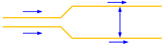
Crosstalk: When parallel traces are too long in circuit design, mutual capacitance and mutual inductance between conductors couple energy to adjacent transmission lines. The following methods can be used to reduce the impact of crosstalk:
- Add safety traces

- Make adjacent traces perpendicular to each other as much as possible in design
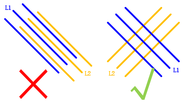
- Increase the spacing between parallel traces after a certain distance
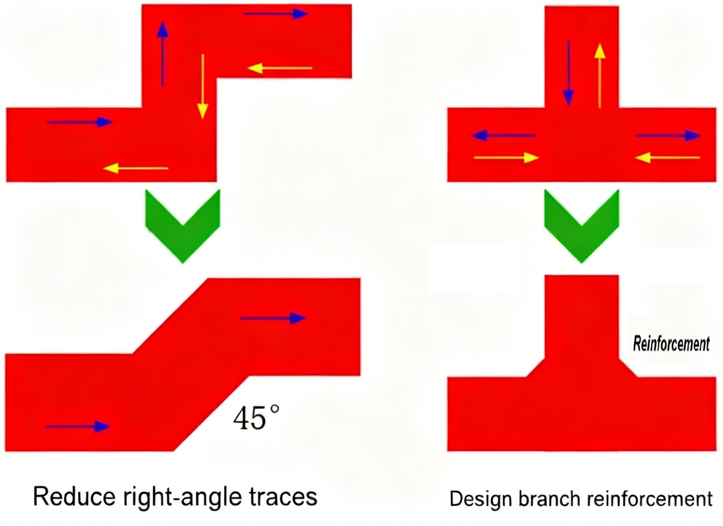
Reflection: Impedance mismatch on transmission lines is caused by too many corners and branches in routing. This can be improved by reducing corners and branches on the line, avoiding right-angle routing, or reinforcing branch lines.
Determination of Grounding Method
Single-point Grounding (for low-frequency circuits): All circuit ground wires are connected to the same point of the common ground, which is simple in wiring and reduces mutual interference of ground loops.
Multi-point Grounding (for multi-layer PCB circuits/high-frequency circuits): All parts of the system are grounded nearby, providing low grounding impedance.
Adding Filter and Bypass Capacitors
Add input/output capacitors to ensure stable input/output voltage.
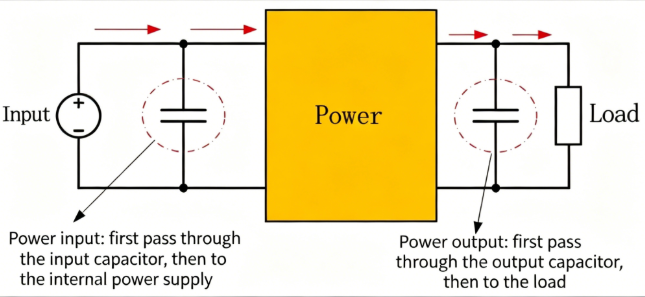
Power input: Pass through the input capacitor first, then enter the power supply.
Power output: Pass through the output capacitor first, then connect to the load.
Add bypass capacitors between the power supply and the IC to ensure stable input voltage and filter out high-frequency noise.
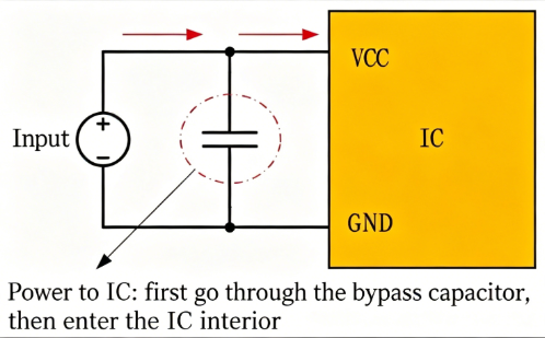
Power supply to IC: Pass through the bypass capacitor first, then enter the IC.
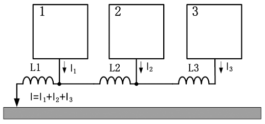
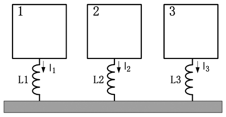
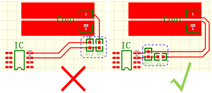
Impedance Position Design
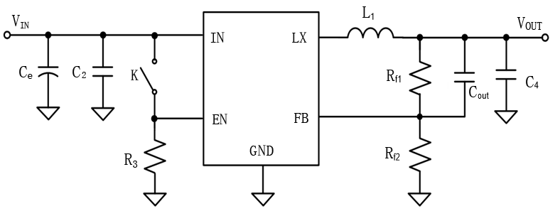
Areas with higher impedance are more susceptible to interference. The following is the PCB impedance position design of a synchronous step-down chip.
PCB Layout Design Techniques
Power/Ground Trace Handling
Even if the routing of the entire PCB is well completed, interference caused by inadequate consideration of power and ground traces will degrade product performance. Widen the power and ground traces as much as possible during routing; preferably, the ground trace is wider than the power trace. The relationship is: Ground trace > Power trace > Signal trace.
For PCBs of digital circuits, wide ground traces can be used to form a loop (i.e., a ground grid) (this method cannot be used for analog circuits). Use large-area copper pours as ground traces, and connect all unused areas on the PCB to ground as ground traces. Alternatively, use a multi-layer PCB with one layer for power and one layer for ground.
Common Grounding of Digital and Analog Circuits
When digital and analog circuits coexist, mutual interference between them must be considered in routing, especially noise interference on ground traces.
Digital circuits have high frequency, and analog circuits have high sensitivity. For signal traces, high-frequency signal traces shall be kept as far away from sensitive analog circuit devices as possible. For ground traces, the entire PCB has only one port for external connection, so the common grounding of digital and analog circuits must be handled inside the PCB. Inside the board, digital ground and analog ground are actually separated and not connected to each other; they are short-connected at only one point at the external connection port of the PCB (such as connectors). Note that there is only one connection point.
Signal Trace Layer Allocation
Routing signal traces on power (ground) layers: When routing on multi-layer PCBs, few traces are left unfinished on signal layers; adding more layers will cause waste, increase production workload, and raise costs accordingly.
To solve this problem, consider routing on power (ground) layers. Prioritize the power layer, followed by the ground layer, to maintain the integrity of the ground layer.
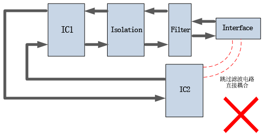
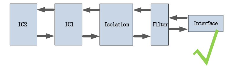
Signal Flow Design
In PCB layout design, strictly follow the principle of linear placement along the signal flow direction, and avoid back-and-forth routing as much as possible.
 About Maxipcb
Maxipcb enables advanced electronic innovation. We deliver one-stop solutions including circuit design, simulation, testing, PCB fabrication, component sourcing and SMT&PCBA assembly, to boost R&D efficiency, speed up mass production and control full-cycle risks. We serve global sectors like communication, industrial automation, aerospace, automotive and semiconductor, jointly forging a safer, connected intelligent future.


 Power input: Pass through the input capacitor first, then enter the power supply.
Power output: Pass through the output capacitor first, then connect to the load.
Power input: Pass through the input capacitor first, then enter the power supply.
Power output: Pass through the output capacitor first, then connect to the load. Power supply to IC: Pass through the bypass capacitor first, then enter the IC.

