Information Required for PCB Design
(1) Schematic diagram: A complete electronic document format that can generate a correct netlist;
(2) Mechanical dimensions: Provide specific positions and orientation identification of positioning devices, as well as identification of specific height limit areas;
(3) BOM list: Mainly to confirm and check the specified package information of components on the schematic diagram;
(4) Wiring guidelines: Descriptions of specific requirements for specific signals, as well as design requirements such as impedance and stack-up.
Basic Processes of PCB Design
- Preliminary Preparation
- PCB Structure Design
- PCB Layout
- Routing
- Routing Optimization and Silkscreen
- Netlist and DRC Check and Structure Check
- PCB Fabrication
The following describes the basic processes of PCB design in detail.
1 Preliminary Preparation
- This includes preparing the component library and schematic diagram. "If you want to do something well, you must first sharpen your tools." To make a good board, in addition to design principles, you must draw well. Before proceeding with PCB design, you must first prepare the component library for the schematic SCH and the component library for PCB (this is the first step - very important). The component library can use the library that comes with Protel, but it is usually difficult to find a suitable library. It is best to complete the component library yourself according to the standard size data of the selected components. In principle, first complete the PCB component library, then the SCH component library. The PCB component library has higher requirements, which directly affects the board assembly; the SCH component library has relatively loose requirements, as long as you pay attention to defining pin attributes and the corresponding relationship with PCB components. Pay attention to the hidden pins in the standard library. Then comes the schematic design, and when it is ready, you can start the PCB design.
- When making the schematic library, pay attention to whether the pins are connected to the input/output PCB board and check the library.
2 PCB Structure Design
In this step, draw the PCB surface in the PCB design environment according to the determined board size and various mechanical positioning, and place the required connectors, buttons/switches, nixie tubes, indicators, inputs and outputs according to the positioning requirements, screw holes, mounting holes, etc., fully consider and determine the wiring area and non-wiring area (for example, the range of screw holes is a non-wiring area).
Special attention should be paid to the actual size of components (occupied area and height), the relative position between components - the size of the space, and the surface where the components are placed to ensure the electrical performance of the circuit board. While ensuring the feasibility and convenience of production and installation, the components should be appropriately modified to make them neat on the premise of being able to reflect the above principles. If the same components are placed neatly and in the same direction, they cannot be placed randomly, which is a patchwork.
3 PCB Layout
- Ensure that the schematic diagram is correct before layout - this is very important! ---- Very important! After the schematic diagram is completed, the check items include: power grid, ground grid, etc.
- When laying out, pay attention to the surface where the components are placed (especially plug-ins, etc.) and the placement method of components (horizontal or vertical placement of through-hole components) to ensure the feasibility and convenience of installation.
- Layout is to place the components on the circuit board. At this time, if all the above preparations are completed, you can generate a netlist on the schematic diagram (Design -> Create Netlist), and then import the netlist on the PCB (Design -> Load Nets). You will see the complete component stack and the flying line prompts for connections between pins, and then you can perform component layout.
The overall layout is based on the following principles: In the layout, you should determine the surface where the components are placed: generally, surface-mount components should be placed on the same side, and through-hole components should be determined according to the specific situation.
- Reasonably divide according to electrical performance, generally divided into: digital circuit area (which generates interference and is resistant to interference), analog circuit area (which is afraid of interference), and power drive area (which is the interference source);
- Circuits that complete the same function should be placed as close as possible, and the components should be adjusted to ensure the simplest connection; at the same time, adjust the relative positions between functional blocks to make the connection between functional blocks the most concise;
- For high-quality components, installation position and installation strength should be considered; heating elements should be placed separately from temperature-sensitive elements, and thermal convection measures should be considered if necessary;
- Clock generators (such as crystals or oscillators) should be as close as possible to the devices that use the clock;
- The layout should be balanced, sparse and orderly, not top-heavy or sunken.
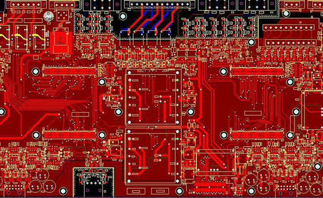
4 Routing
Routing is the most important process in the entire PCB design, which will directly affect the performance of the PCB.
In the PCB design process, routing is generally divided into three levels:
The first is connection, which is the most basic requirement of PCB design. If there are no laid lines and the lines are flying, it will be an unqualified board. It can be said that it has not even started.
The second is the satisfaction of electrical performance, which is an indicator to measure the qualification of a printed circuit board. This is to carefully adjust the routing after connection to achieve the best electrical performance, followed by aesthetics.
If your wiring is connected and there is no place that affects electrical performance, but at a glance, there are many messy and colorful lines, then no matter how good your electrical performance is, it will still look like a piece of garbage to others. This brings great inconvenience to testing and maintenance. The wiring should be neat and uniform, and there should be no messy lines. These must be achieved while ensuring electrical performance and meeting other personalized requirements.
Routing is mainly carried out according to the following principles:
- Under normal circumstances, power lines and ground lines should be routed first to ensure the electrical performance of the circuit board. Within these conditions, try to widen the width of power and ground lines. The ground line is better than the power line. Their relationship is: ground line > power line > signal line. Usually, the signal line width is 0.2~0.3mm. The thinnest width can reach 0.05~0.07mm, and the power line is generally 1.2~2.5mm. For digital circuit PCBs, wide ground lines can be used to form loops for forming a ground grid (the ground of analog circuits cannot be used like this);
- Pre-process lines with higher requirements (such as high-frequency lines). The edges of the input and output terminals should avoid adjacent parallelism to avoid reflection interference. If necessary, add ground lines, and the wiring of two adjacent layers should be perpendicular to each other, as parallelism is prone to parasitic coupling;
- The oscillator shell is grounded, and the clock line should be as short as possible and cannot be led everywhere. Below the clock oscillation circuit and the special high-speed logic circuit part, the ground area should be increased, and other signal lines should not be used to make the surrounding electric field close to zero;
- Use 45° broken lines as much as possible, do not use 90° broken lines to reduce the radiation of high-frequency signals; (high-speed lines use double arcs);
- Do not form loops on any signal lines. If unavoidable, the loop should be as small as possible; the number of vias for signal lines should be as small as possible;
- Key lines should be as short and thick as possible, and add protection on both sides;
- When transmitting sensitive signals and noise field band signals through flat cables, they should be extracted by "ground-signal-ground";
- Test points should be reserved for key signals to facilitate debugging, production and maintenance testing;
- After completing the schematic routing, optimize the routing. At the same time, after the initial netlist check and DRC check are correct, perform grounding of the wireless area, use a large-area copper layer as the ground line, and connect all unused areas on the printed circuit board to the ground as the ground. Or make a multi-layer board, with the power supply and ground each occupying one layer.
5 Add Teardrops
A teardrop is a teardrop-shaped connection between a pad and a line or between a line and a via. The purpose of setting teardrops is to avoid disconnection at the contact points between conductors and pads or between conductors and vias when the circuit board is subjected to large external forces. In addition, the setting of teardrops can make PCB circuit boards look more beautiful.
In circuit board design, to make pads stronger and prevent disconnection between pads and wires during mechanical board manufacturing, a transition zone made of copper film is usually arranged between pads and wires, shaped like a teardrop, hence commonly called teardrop.
6 Inspection
In turn, the first inspection is to check the Keepout layer, top layer, bottom layer, top overlay and bottom overlay.
Electrical rule check: vias (0 vias - very incredible; 0.8 boundary line), whether there is a broken netlist, minimum spacing (10mil), short circuit (analyze each parameter one by one)
Power line and ground line check - interference. (Filter capacitors should be close to the chip)
After completing the PCB, reload the netlist mark to check whether the netlist has been modified - it can work normally.
After the PCB is completed, check the lines of the core equipment to ensure accuracy.
About MaxipcbMaxipcb enables advanced electronic innovation. We deliver one-stop solutions including circuit design, simulation, testing, PCB fabrication, component sourcing and SMT&PCBA assembly, to boost R&D efficiency, speed up mass production and control full-cycle risks. We serve global sectors like communication, industrial automation, aerospace, automotive and semiconductor, jointly forging a safer, connected intelligent future.

